Background
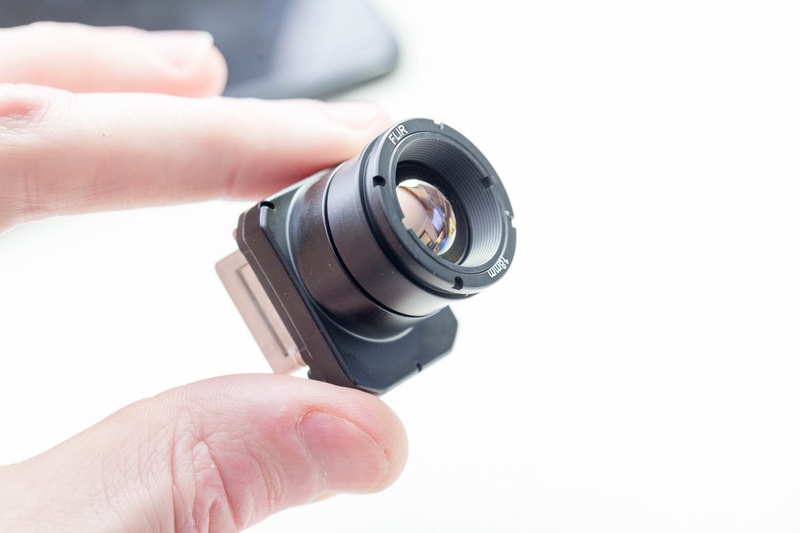
FLIR has recently released a new OEM thermal Camera core. The Boson. These cores are self contained units that handle all the complexities of thermal imaging. They contain the thermal image sensor itself, a NUC/FFC shutter, and a lens assembly capable of focusing thermal energy. They also contain control electronics that present a standard CMOS style image sensor parallel interface. (DATA + CLK + HSYNC/VSYNC).
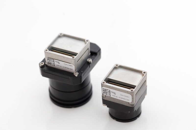
Having used the previous Thermal core from FLIR (The Tau 2) at work in project, our local distributor sent us some Boson cores to have around for integration. These unfortunately sat on our shelf for a few months. I wanted to learn how to design projects with FPGAs, so I decided to create an FPGA based product to capture the data stream from the Boson core into a usable format.
Design
Prototype v1
This is my very first FPGA project, I had used FPGAs before in a uni class on Digital Electronics. I had also learnt about the RISCV CPU architecture in Computer Architecture. But had never designed an FPGA into a project. I had just listened to an episode of the Amp Hour with Clifford Wolf, explaining the Lattice iCE40 open source toolchain: icestorm. So naturally I started there. (Also Naturally I picked the only variant in the iCE40 family that is not compatible with icestom. Still supported by lattices’ tools.)
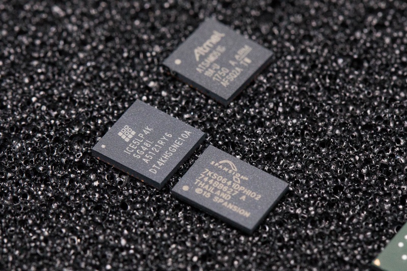
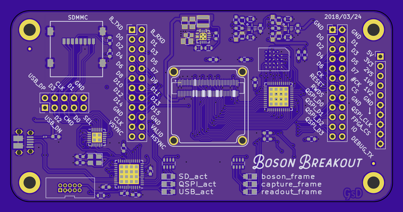
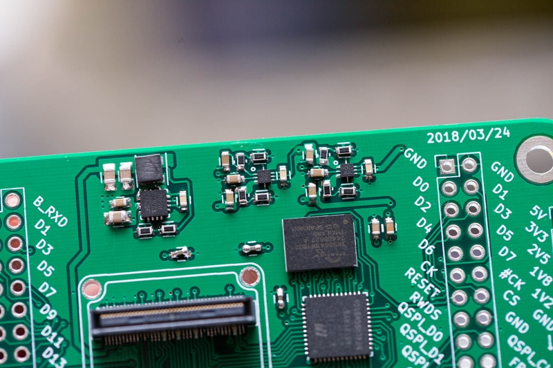
I crawled through the datasheets for the iCE40 Family and the variant I picked the iCE5LP4K, this was available in an easy to solder QFN 48. I decided to “simplify” the FPGA work by basically creating a large FIFO. This would capture a frame from the high speed datastream of the camera into some external RAM, then a microcontroller could read this data at its own pace and save it to an SD card. This probably would have worked, but I never developed the code for this completely. I had already started developing v2 with a larger FPGA on a smaller PCB. That will be talked about in part 2.
The RAM I chose was 64Mbit of hyperRAM. HyperRAM is self refreshing DRAM, which is refered to as Pseudo SRAM (PSRAM). This provides the high density benefits of DRAM with the simplicity of SRAM. It uses a 12 wire Interface bus which uses a 8bit DDR data bus and control signals. Due to its nature it’s a champ at long bursts of data. Perfect for the streamed data from the camera.
I chose the SAMD51 as a microcontroller to handle the SD + FAT stuff mostly because I had just used them in another project. :) But they do feature a true SDMMC 4 bit interface which is essential to get any decent performance from an SD card.
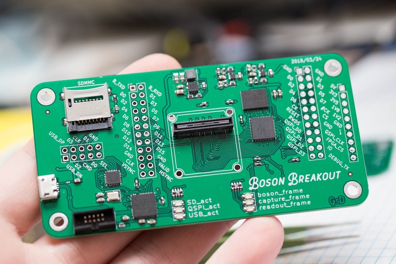
Hardware Assembly
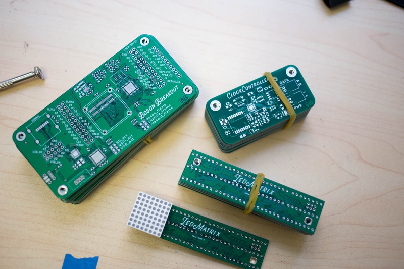
This is the part of a project I enjoy the most. I was able to hand assemble this prototype with a soldering iron and a hot air setup. (Tip: use lots of flux). The PCBs arrived from PCBWay, I had all my parts from Mouser/Digikey, I was ready to assemble.
Some comically small parts on this board are these voltage regulators, They are adjustable dual LDOs, I used 0603 caps/resistors which individually are almost larger than the chip. Still an easy job to assemble with the right tools and some practice.
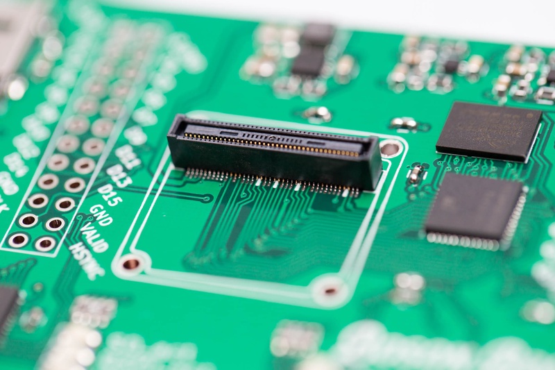
One interesting point of this prototype was the discovery I could make a custom footprint for the connector in KiCad, this custom version removes alot of pins that are unused in this application. This enables me to route out the signals all on the top layer. Because these pins may still have a voltage/signal present on them it is essential that a soldermask is present underneath the repurposed pins.
Firmware
I designed the FPGA to be configured through a slave device of the samd51. This took too long to get working, by the time I had it working and had started working on the verilog the new prototype had arrived, and I decide to leave this project. It had served as a great first step in getting started with FPGAs and had given me added confidence with the tools and workflow.
However I did develop a simple hyperRAM interface in a verilog simulator, when I tried it on the real hardware I discovered a serious bug…
Errata
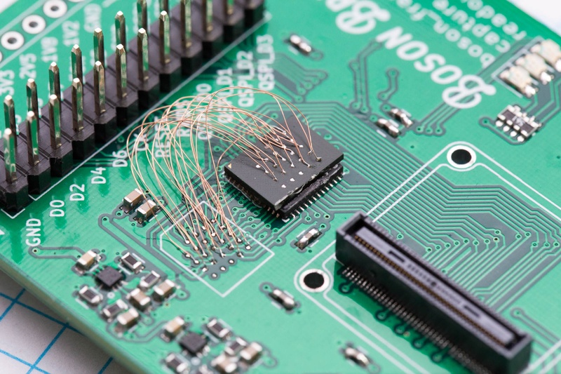
In my haste to develop an entire PCB with new components. I had mislabelled the coordinates on the BGA footprint. This required me to perform the following rework. Surprisingly this does actually work. My code that tested this was only running at 12MHz bus speed. But I’m still impressed with my own job. I did this without the aid of a microscope (I have since bought a microscope.)
In Part 2 I take a look at the hardware behind version 2 prototype!