In this part I want to talk about the firmware, or code, this device will need in order to operate as I want.
But before I get to that lets take a quick step backwards to some back of the envelope engineering I did when I was thinking about the hardware required to save an image from the camera.
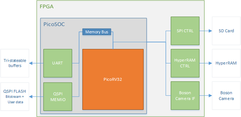
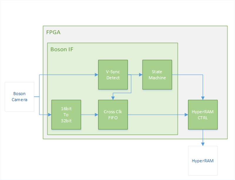
Data Flow
The Boson is designed to stream images out automatically, the camera has a control interface, but you cannot simply ask it to “snap” a photo, and read it out byte by byte. Instead it just rudely spews out data. It has a 16bit bus running with a 13.5MHz pixel clock. This equates to a bus speed of 27MByte/s. Luckily for us pixel data on this bus comes in bursts, before and after each line of valid data there is a gap and after every line in a frame has been transmitted there is a few lines blank. These are Horizontal and vertical blanking periods designed to give electronics some time to process the information. (My understanding is that originally these were to give CRT screens time to energize coils and steer the electron beam back to be ready for the start of the next row. But they are still common place in many video formats.)
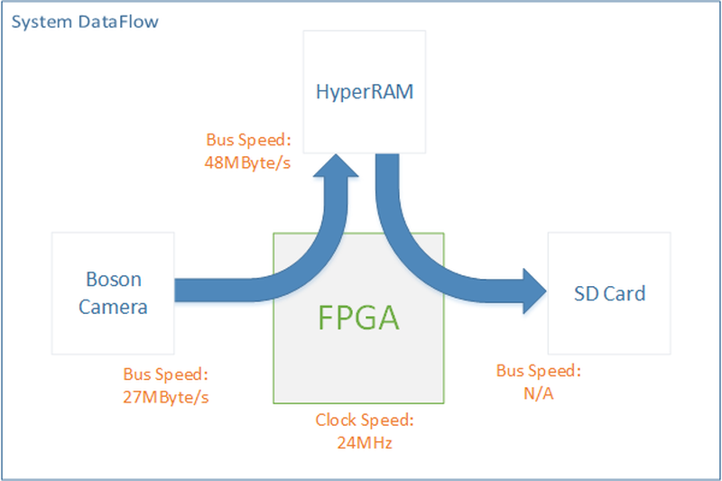
I decided to add high speed RAM to the design in order to ensure I could reliably capture the video frame. I have used SD cards in the past and it is pretty common place for them to have variable delays when writing data blocks to them as they perform various internal operations. If I could get away with bypassing the RAM in the final design, great, but I still wanted it in the hardware.
One benefit of using the RAM is that it doesn’t matter what speed the SD card is running at – this makes life easier. I can develop the modules that are needed to run the system then leave as much optimization till the end.
Verilog & PicoSoC
Code that describes hardware. As mentioned this is my first FPGA project. I had already selected the iCE40HX8K as it was the largest ICE40 in the smallest package. This particular FPGA has 8k LUTs. I didn’t know how many LUTs my design would require. Is 8k a lot? What is a LUT? I’m not going to go into FPGA basics, but from my experience 8k is enough to implement a RISCV 32 bit processor and a handful of basic peripherals. It is enough to get your feet wet in a real FPGA project!
I had chosen the ICE40 as a target device because I was reading about a free open source FPGA tool-chain ice-storm. I followed the guides and examples and got a LED blinking on the back of my board! This project was on it’s feet. But I was still a bit outside my comfort zone.
Claire Xen is the creator of the icestorm project. She also created a lightweight RISCV processor called picorv32. More importantly for me (A verilog newbie) she packaged this into PicoSoC.
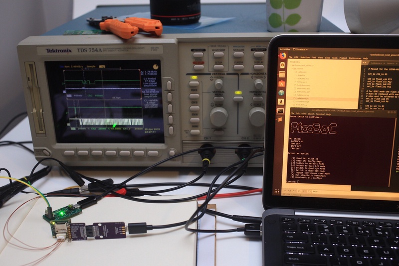
PicoSoC is a combination of the RISCV CPU picorv32, a flash memory controller for reading in program data, some SRAM, and a UART serial port. Also an example built on the Lattice HX8K evaluation board! The processor let you write C code and using memory mapped register directly control and monitor bits in your custom hardware. it was a perfect way for me to ease into FPGA design. PicoSoC has some great step by step instructions in order to compile and get it loaded, one of the steps is downloading and compiling a RISCV variant of GCC. This went smoothly but was the slowest port (~4 hours on my slow laptop.) The wait was worth it, because after it finished I had PicoSoC loaded and running on my custom hardware. The UART link to the PC gives you a very simple text console which I think is perfect for adding to and modifying in firmware. (Love the PicoSoC splash screen btw Clifford!)
Think Modular
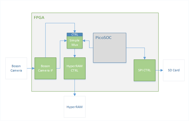
Verilog is constructed as a very hierarchical language. Which means when developing systems for FPGAs you should be thinking about modules, how can you split your design into modular blocks that fit together. I envisioned a system as shown above, I had now validated that the FPGA was functioning, SPI FLASH and programming worked, and my User I/O and LED worked. I wanted to write some logic to test the SD card, HyperRAM, and Boson Interface. Any of these could have a hardware bug in the PCB design that could render this prototype useless.
Boson IF
I wrote the Boson Interface first as a basic FIFO, using commands in the SoC’s firmware I was able to reset the FIFO and print out 16 values that had appeared from the camera over serial. This with a combination of holding my hand in front of the camera indicated that data was been read correctly from the camera.
HyperRAM
I had started working on a hyperRAM module with my first prototype hardware. However I didn’t really understand what interfaces I would need to support the burst style data that the RAM needs in order to sustain it’s read speeds. At this time I saw Kevin Hubbard from Black Mesa labs had just released an open source HyperRAM library, His library relies on dividing the clock rate by 4 to properly generate the DDR signal timings without having to worry about device specific PLLs. With a bit of reading though his very well documented code I was able to add his module to the PicoSoC system bus and test the RAM using some simple functions in C.
Micro SD & FAT
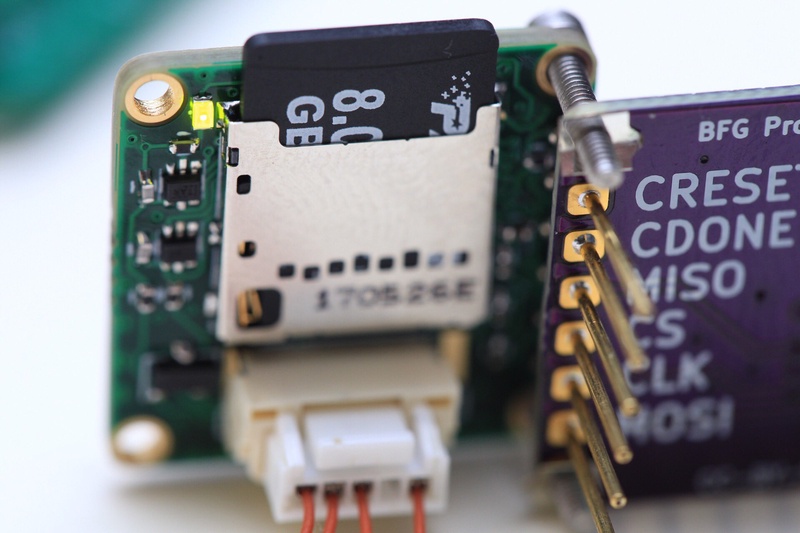
The biggest benefit of using a softcore processor in my design in my opinion was the ability to leverage existing open source software projects. FatFs is one of those projects, I’ve used it on countless projects in the past. The example projects include a “barebones” implementation of the low level control using bit-banged IO. In order to get this to work I just had to extend the GPIO registers from write only to R/W and map them to the SD card pinout in verilog. With those small changes* I was able to write a file to the SD card!
I spent an entire evening scratching my head as to why FatFs wasn’t working. As soon as I looked at the memory-map output from GCC I worked out why, I think one of the goals of PicoSoC is to be simple enough to get up and running fast. Because of this the example firmware (what my code was based off) only utilized the RAM on the stack, the linker never declared where to store static/global variables, and the startup code never initialized these. I did a few unspeakable linker-hacks to get it to work initally. A better solution is to use the code provided by Miodrag Milanović, Who did a great job porting microPython to the picoSoC.
Pick Your Battles
Now with each hardware component tested to be working I knew the hardware should be capable of capturing an image from the camera, I just had to tell it how to do it.
My idea for a simple capture sequence is as follows:
- On powerup Boson IF module has control over the HyperRAM. The CPU tries to access the HyperRAM and becomes stalled.
- The Boson IF waits for a Vsync pulse to synchronize with the image.
- It captures an image through a Dual-clock FIFO. (Boson Camera Controls the pixel clock)
- A small state-machine empties the FIFO.
- After 3202562 bytes the state-machine in Boson IF releases the HyperRAM.
- CPU takes over and using FatFS writes an image to the SD card.
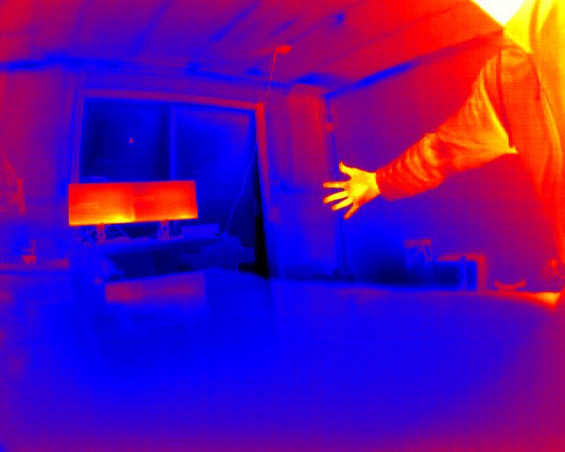
To my surprise this worked! Not ideal though, you had to restart the camera to take a new photo, the SD card was still slow, and it would over-write the last photo you took.

- You can see a few errors with this photo, firstly I miss-judged what the focal distance would see.
- There is a 2 pixel band on the left image that’s actually pixels from start of the next line.
- I messed up the endian-ness so every pair of pixels is flipped.
- Still a success!!
Optimise When Ready
I systematically went through and added performance to each module.
- HyperRAM got updated to make use of the DDR IO and PLL in the ICE40.
- SD driver got updated to a hardware SPI module running at 12MHz.
- Control registers added to the Boson IF to enable capture through the picoSoC terminal.
- Lastly I added a simple DMA to copy data from the HyperRAM out into the SD card without requiring the CPU. This greatly improved performance.
I reduced the time to save an 320x256 image from ~12s to ~0.3s.
Moving Forward
At this point I’ve run out of space inside the ICE40HX8K. I’m sure there is room to optimise the current design, but it is very difficult to add extra features. In order to push the performance even further I will need to swap the SD SPI driver for a real SD 4-bit interface. There are a few open source versions but none of them fit. Time to look for a bigger FPGA?
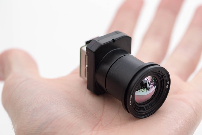
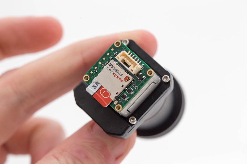
Up to this point I had I had been working with a Boson 320x256 9Hz I’ve borrowed from work. GroupGets a FLIR distributor among other things offered to send me a Boson 640x512 60Hz model! Amazing! If you’re interested in picking up a Boson Camera check out their range!
Unfortunately the Camera running at 60Hz outputs data too fast for the logic in my HX8K board to keep up with. It’s pixel clock is 27MHz at 60Hz which corresponds to a 54MByte/s bus speed. The FIFO can capture this but my HyperRAM bus is not able to sustain a data rate to be ready by the next line. But by enabling the average in the camera the frame rate is reduced to 30Hz and the clock brought down to 13.5MHz, with some small tweaks I was able to capture this frame. (95 degree FOV is VERY wide!)
I have plans to create an updated version featuring a more power processor capable of handling both the Boson 320 and Boson 640. Stay tuned for more details about this in Part 4!
Here is a teaser! 😉