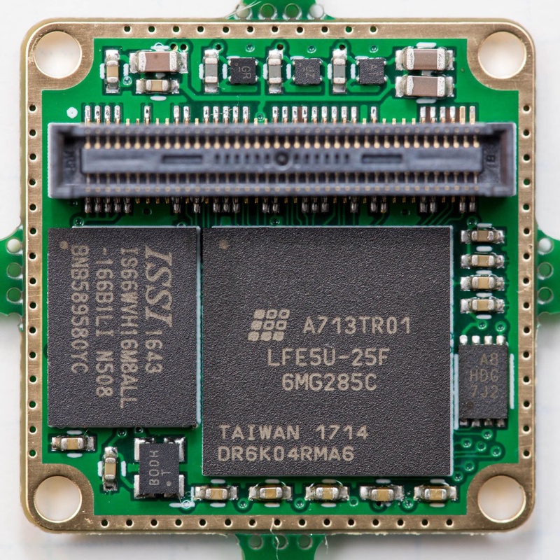
The new hardware for the Boson Frame Grabber will be based around the Lattice ECP5 family. Lattice make available a free IDE for this FPGA assuming you are not using a model with embedded SERDES. Since we are not, it’s perfect for our application.
The ECP5 is classified as a high-performance low power FPGA. there are variants available with 2.5/5Gb/s SERDES. The biggest feature for this application is it is available in a 8x8mm 285pin csBGA package. Additionally, the ECP5 is available in 12K,25K,45K,85K LUT variants. Given that my last design was approaching 8K LUTs, I suspect a design will fit in 12K. But the minimal price increase for the 25K variant makes it a pretty good choice.
Design
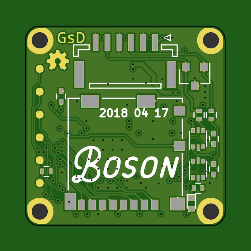
The design PCB layout of this new version is derived from the v1_01. With the following changes:
- Switched out the iCE40HX for an ECP5 in csBGA 285 package.
- Changed the LDOs. Now separate tiny LDOs for each 1.1, 1.8, 2.5v supplies.
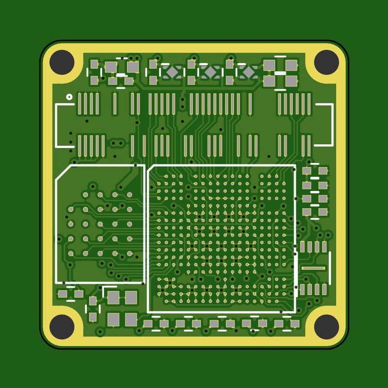
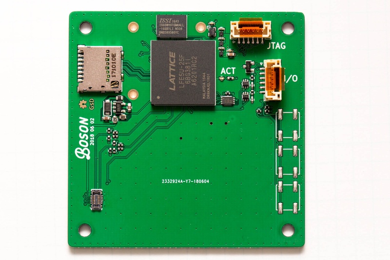
The HyperRAM, FLASH, IO level-shifters, JTAG points, Oscillator are all the same. I’m still using the altered footprint for the Boson connector, this definitely helps with routing. The extra width from the ECP5 and the extra pins along the top also help with routing the 16bit parallel bus from the camera into the FPGA.
You can see the updated FPGA page of the schematic below. I’m using around 60 out of the 118 available PIO pins on this package. I tried to constrain high-speed buses like the SD card and HyperRAM to their own bank. But I don’t think that’s particularly important at the speeds I’m working within this design. What is important is ensuring that devices connected to a particular bank are at the right IOVDD level.
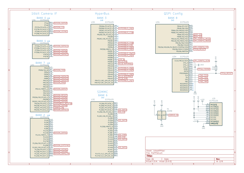
We have 2 different IO voltages in this design
- 1.8V - HyperRAM, Boson, Oscillator, I/O
- 3.3V - SDMMC, FLASH
Because I had specifically used level-shifting Tri-stateable Buffers for the two external IO ports, I’m easily able to control them from a 1.8V IO bank.
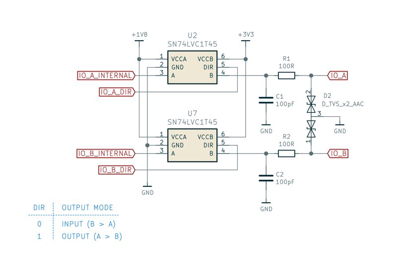
The main reason for using these buffers is to ensure that the low voltage sensitive IO pins of the FPGA are somewhat protected from external signals, The buffers used are SN74LVC1T45’s They will tolerate voltages up to 7V and retain their high-impedance state even when they are not powered.
With these Tri-stable buffers, it’s often useful to write on your schematic what the DIR pin actually does. Often they can take an inverted input. Writing this stuff on a schematic it is a lot easier to see than pulling up the datasheet again if you forget or want to double check.
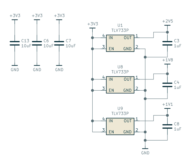
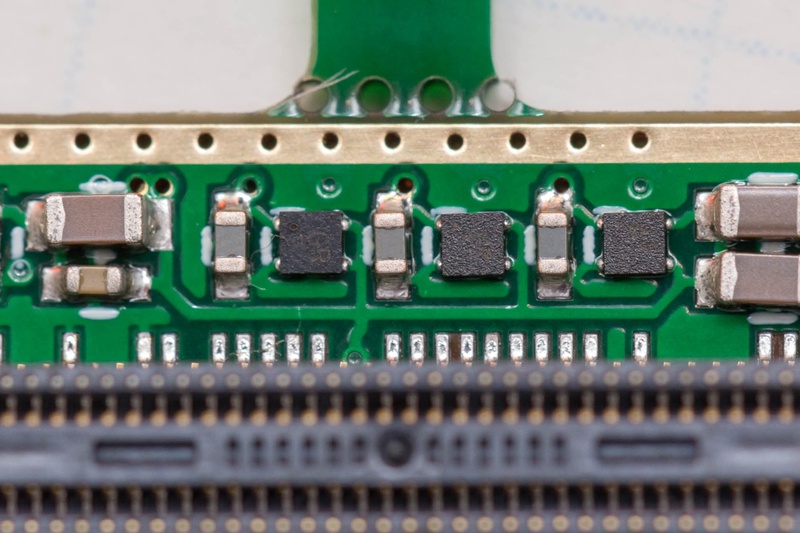
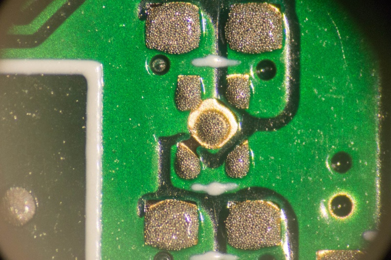
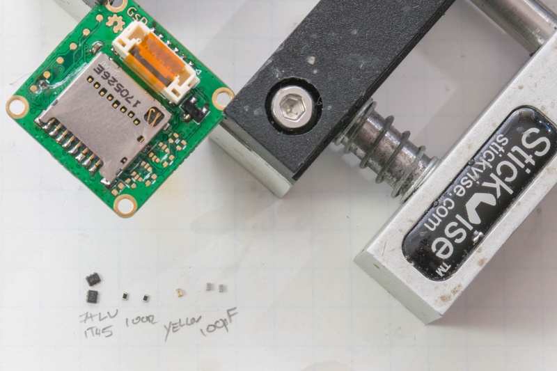
I’ll mention the LDOs I used again. I used TLV733P parts, but it’s a jelly bean part available from many different manufacturers. The package I need is the XSON style 1x1mm package, very challenging to solder. But the small size is essential to fitting everything on my 21x21mm PCB. For reference, the capacitors next the regulators between are 0402!! Yes, they’re small. I’ve seen raw sugar crystals bigger than these regulators.
Check Leadtimes (I designed a v1_03 PCB)
One thing I did not check until after I had ordered wy PCBs was the availability of the ECP5 in csBGA 285 package. It turns out there was either a bit of a shortage, or it’s not a standard stocking part. Lattice lists an 8 week lead time, luckily from lattice you can buy singles with this lead time for prototypes. But from some distributors request you order an entire tray or 168 parts!
Because I was impatient, I decided to create a testing board using an in-stock package of the part. Here is that board. I made it bigger to support an LCD screen.
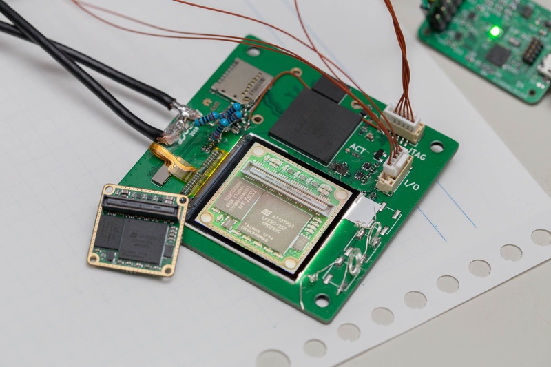
This board is v1_03 in the github project. But it has an errata list longer than my arm. All caused by rushing the design over one weekend. I managed to get it mostly working, but it will never support auto-configuration from FLASH. So in order to run it, you are required to load a bitstream through JTAG.
What ended up happening is that the day I assembled this prototype big-board, I found that Lattice had stock of one variant of the ECP in csBGA 285 package. This ended up being around 2 weeks out of the quoted 8 weeks lead time.
v1_02 (But this time with parts)
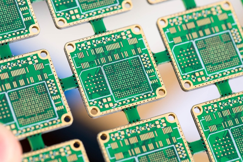
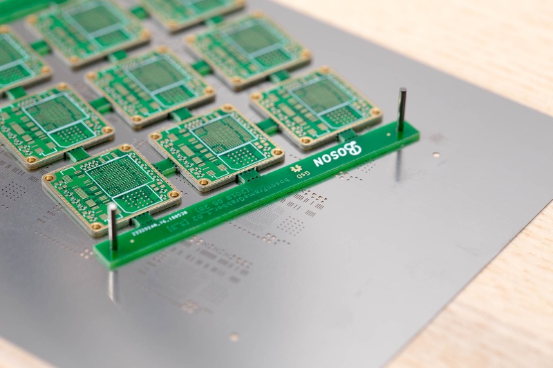
With parts in hand, the assembly proceeded without a hitch. I made use of a stencil from OSH Stencils. This is the first time I’ve attempted this. But I added holes to my edge rails on my PCB panel, and spec’d corresponding holes in the stencil. Using some small Steel pins makes stencil alignment PERFECT!
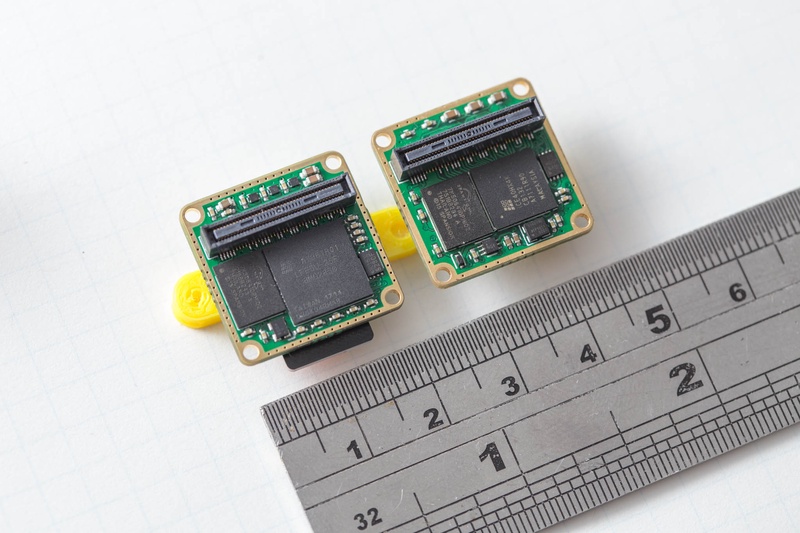
When I designed the iCE40 Version I thought I had packed the PCB, but this is even denser. I’m very proud of my efforts to design this board and still remain within a “standard” PCB 4 layer process.
I am still hand-assembling the rear-side components. Just use lots of flux, and a fine tipped iron with a flat edge. Lastly, a family shot of v1_01 next to its superior v1_02 hardware.
In the next part I’ll finally describe the firmware* design. Hopefully, I can this hardware to work. (Even if doesn’t work, it looks great!)
(*Is Verilog firmware? That’s something I’m not clear about.)
Update:
I’ve been informed that RTL is often referred to as “Gateware”. Which seems quite fitting