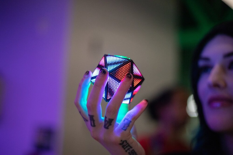
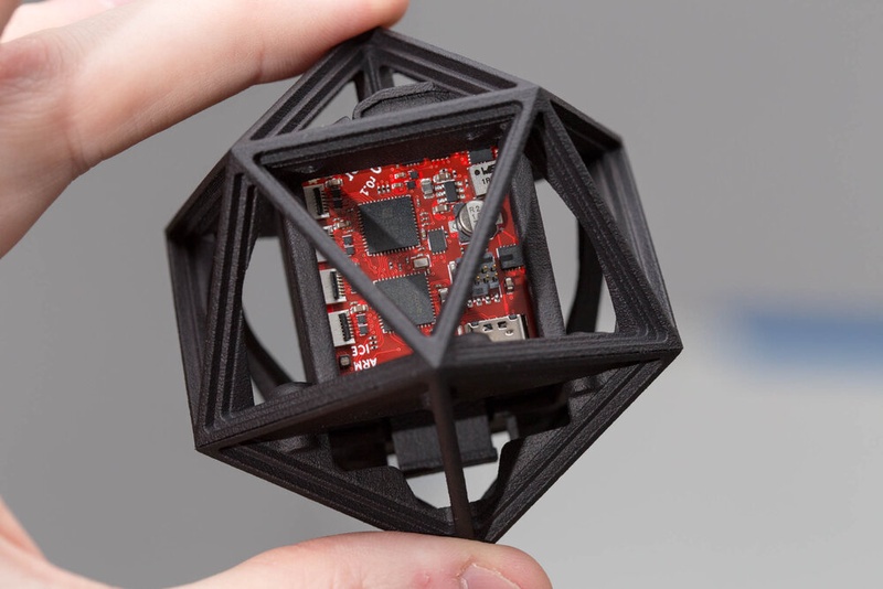
A tennis ball sized, 20 sided, LED clad, regular polyhedron
Introduction
The major challenge of making a smaller LED cube in my opinion is the LED panels. Commercially available panels are designed for video walls and typically made at 64x64 pixel as a minimum size. This seems to be a good trade off between cost/complexity/light efficiency. On my previous project mini-led-cube I had overcome one of the major hurdles of creating a smaller cube, because I had designed and built my own custom high density* LED panels.
(*high density: less than 2.5 mm pixel pitch)
So what next? I could make it smaller, improve the controller, improve the firmware. What about adding more sides?
Inspiration came from this origami figure that I’d built many years ago and that has been sitting on my shelf.
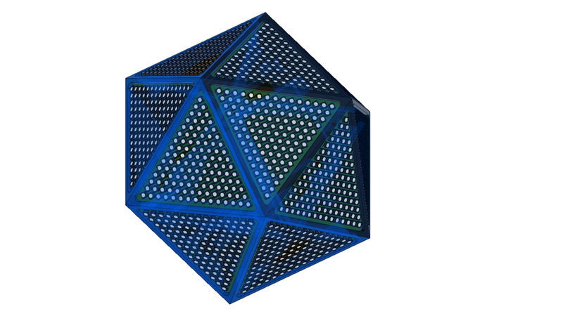
I’d never seen a LED icosahedron before…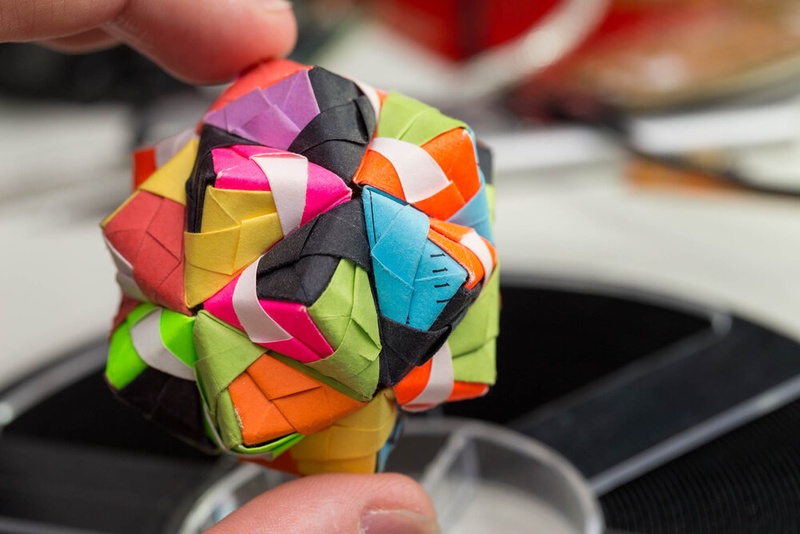
Design decisions
I started by thinking about at a birds-eye view of the project, what major aspects there would be. What I know I wanted from a design point of view, and what I still had to work out. Engineering projects are always about problem-solving, so it helps to have a clear view of the problems that lie ahead of you.
Panels
- I would need to design a LED panel that was compact and contained all the electronics.
- This panel would be in the shape of an equilateral triangle, and have a method to connect it easily to other panels to form a chain.
- How would I arrange the LEDs on the surface of each panel to assist in routing. Knowing the panels were at different angles I would like them them to align no matter what orientation they were fitted in. 120 degree symmetry.
Enclosure
- How will the panels be held together with minimal bezels
- 3d printing is an obvious answer since this enclosure has lots of weird angles
- Probably a 3d printing service that does resin or nylon
- Resin is discounted due to personal experiences with in being brittle and discolouring over time
- Want a black material, so the case isn’t noticeable
- Total overall size? Thinking tennis ball/rubiks cube sized to match the cube
Controller
- Can make use of controller design for the cube, will need to be re-designed to fit in the smaller form-factor
Power
- How will this be powered? 18650. RC hobby LiPo cells?
- I want to be able to carry this on a plane, will probably require something a little bit more friendly looking.
Timeline
- I’m super late in writing this blog post. I started thinking about this project in September 2019, and want it ready to take to supercon 2019. Which I was leaving my lab on the 2nd of November. So I had a little under 2 months to pull it off.
Design Stage
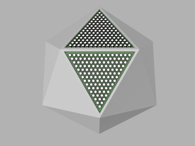
At this point I had an idea in my head about what I wanted the device to look like. However there were no hard or fixed numbers yet. So I knew I needed to work out the dimensions of each panel first. I did this in my 3d CAD of choice, fusion 360. I looked up a tutorial about how to model an icosahedron, which was more complex than you might imagine. Once modeled, I scaled it to be roughly tennis ball sized, this left me with a triangular face with sides of 42mm. From this I inset slightly to give room for the panels to be sunken down into the enclosure.
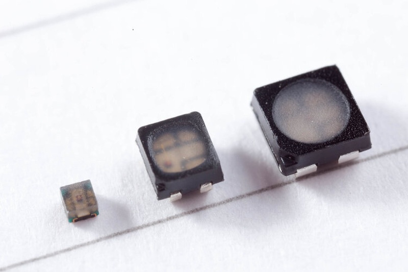
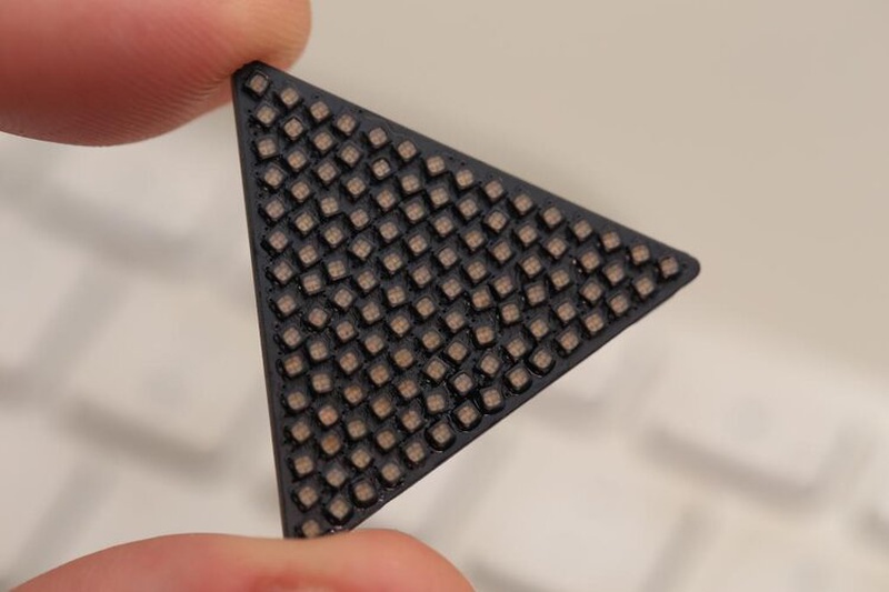
I had used 2x2mm LEDs for the cube, and knew they came in a smaller variant, 1.5x1.5mm. These would be perfect. They feature a black casing that helps highlight the round lens on the top. This is particularly important because as you move this around, some panels the LEDs might be rotated, but so long as round opening is in the same location you generally won’t notice.
You can get smaller LEDs, however these create some more challenges. I need to be able to route this board easily and didn’t want to start using HDI features. (Blind/buried vias). To achieve this a trace needs to be run through the middle fo the LED pads, this isn’t possible with these smaller 1x1mm or 0.7x0.7mm RGB LEDs. Secondly because they don’t feature the black enclosure I was worried that light bleed between pixels would be bad.
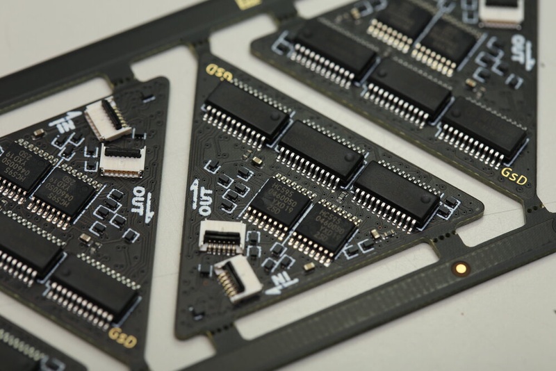
Based on the experience I had with the cube I knew I could create a matrix arrangement for the LEDs, and make use of the 16bit constant-current LED drivers + 595/PMOS source drivers.
The TLC59025 sink drivers are set to a single current for the entire 16bits it’s a requirement to use 3, one each for R,G,B. This is because each colour will require a slightly different current to produce a nice white. I say “style” because you can find multiple pin compatible drivers. lcsc sell a few that have Chinese only datasheets, but because they’re designed as drop-in replacements that isn’t an issue. You can save quite a bit of money using these. Especially given I needed to use 60 of these in the project.
These drivers only turn ON/OFF they don’t handle any greyscale control themselves. Because of this you do want to connect both the LATCH and BLANK signals. This enables you to clock new data in while current data is being displayed. As well as control the exact interval data is displayed for. This and some FPGA logic is what enables high refresh rate greyscale control.
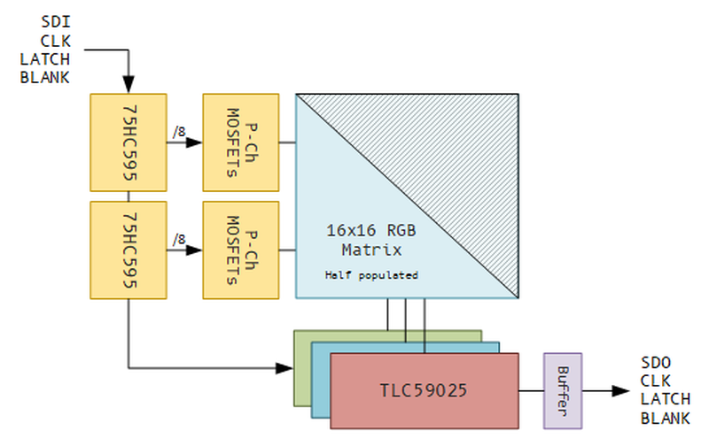
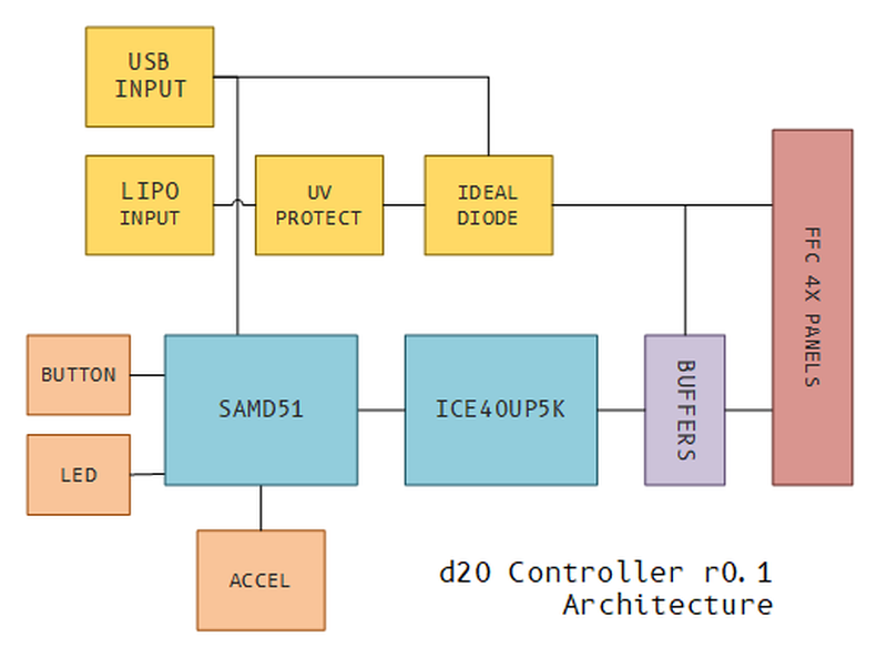
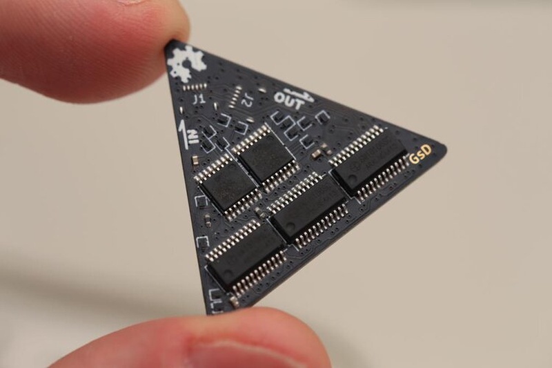
The architecture is shown above. There are a few interesting observations.
- I placed everything in a single serial string. This represents 64bits from input to output, and is primarily to reduce the pin count of the connectors, and hence the internal wiring.
- r0.1 boards did not have buffers, but I noticed after 3 panels there was some glitches. So I added those.
- I’ve include enough electronics to drive an entire 16x16 matrix, but only populate a triangular portion of it. This GREATLY helps with signal routing. I’m already at 4L to route power/signals on inner layers, but I tried routing it with just a single 8bit source driver, and failed.
- I opted for 6-pin 0.5mm pitch flat flex cables. These were actually a little bit tricky to find, ended up buying various lengths from an aliexpress seller.
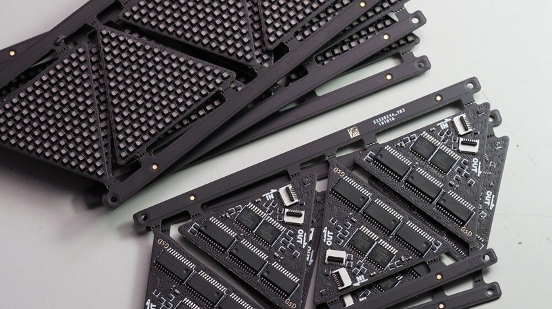
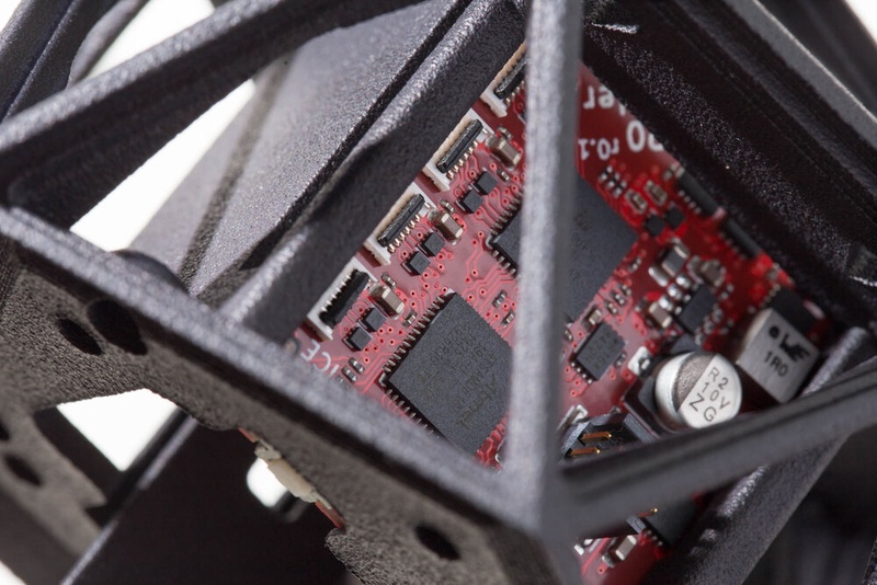
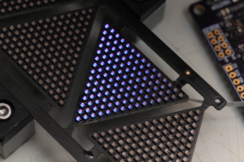
With the space available I am able to fit a triangular array of LEDs with 15 pixels across the base and 15 pixels high. this comes out to 120 LEDs per side.
With 20 sides this results in 2400 LEDs total. This will be fun to hand place! but I’ll leave that for future Greg to worry about.
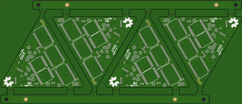
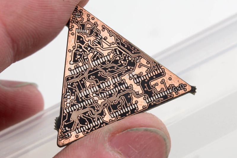
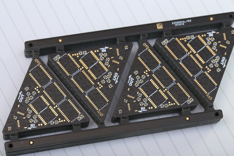
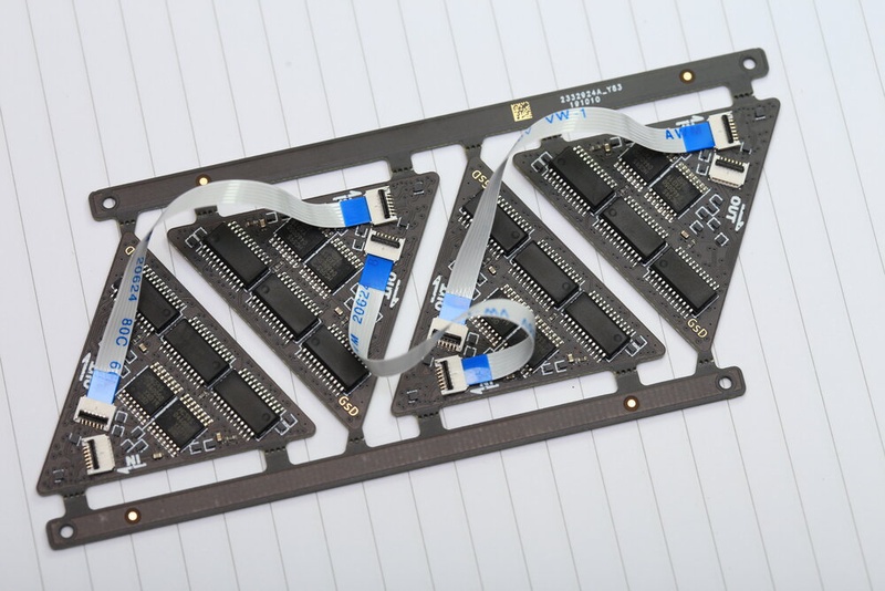
Panel r0.1
Shown above is the panel I sent off to have made at JLC PCB. (https://jlcpcb.com/) They were kind enough to provide free PCBs and stencils for this project.
I placed this order on the 12th of September.

The boards arrived ~1 week later. And they looked good on the surface. I went to assemble one, and when trying to determine the LED orientation I discovered a fatal flaw. I had the footprint rotated 90 degrees. (-___-)
I attempted to assemble a board bey placing LEDs at 90 degrees, but ultimately this was a failure, the pads look reasonably symmetrical, but they’re not exactly. So when placing the LEDs at 90 degrees there isn’t great surface tension during reflow to pull them into alignment. Yep, that alignment looks pretty ugly.
Also worth noting that because I did not have the FFC cables or connectors at this point, and I had not written the code to drive the display, I didn’t even attempt at powering this on. Maybe you can sense the foreshadowing, in this observation.
Panels Take two
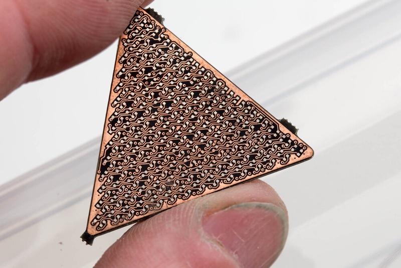
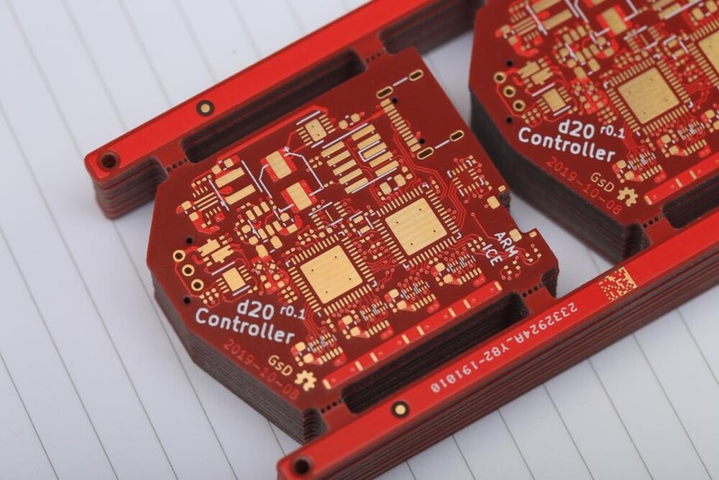
Everything else about the panels seemed fine at that time, so I quickly adjusted the footprint. ripped up the top layer and re-routed. I had a bit of creative energy/motivation left at this point so I added 2 little dual input buffers to the design, This helps isolate each panel from the next. Particularly the clock line, and removes some glitches I was seeing on the cube design. With the routing complete I placed the order again with JLC, this time I just payed for the boards myself, because I was now on a tighter deadline and I didn’t feel like asking for more free stuff because of a dumb mistake on my end.
I placed this order on the 10th of October
Enclosure
Let’s switch gears to the enclosure, with a design for the panels done I can export a 3d model from KiCad and start looking at how they’ll be integrated into an enclosure. I did have to model up a custom LED. Which was very useful to see how everything would be fitting.
The panels fit great, and the bezels looked thick enough to be manufacturable, now it was just a matter of going through and cutting away as much of the enclosure as possible. Nylon MJF prints are priced by they’re total size and how much total material ends up in the final print.
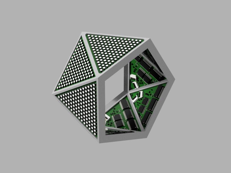
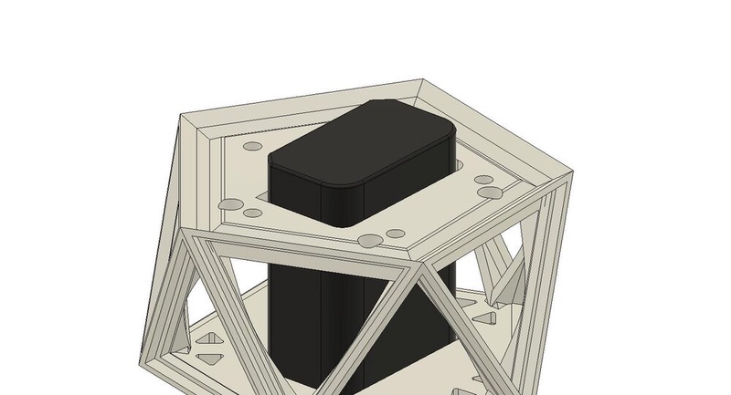
With regard to powering the device I managed to fit a Sony mirror-less camera battery in the enclosure, and even more surprising I found a compatible 3-pin terminal that actually fit the battery! (That’s one of the challenges of using this style of battery).
I needed a way to insert/remove the battery, and I’d determined it was easiest to remove a section of the icosahedron with 5 panels in it, these 5 panels would have a single ribbon cable running between it and the base. The sections would have asymmetric locking features and magnets, so it could be securely fastened and removed.
could not find imageI even tried to be clever and add locking features to the 3d print to retain the controller PCB. Fusions “look-at” [face] option and the section-analysis were vital in getting this designed.
With the two halves designed, and checked multiple times over a few days I was ready to order them. I don’t really know too many options around for quickly prototyping a Nylon MJF part, so I just opted for shapeways. I opted for their higher detail service, with express options. The order totalled $167.68 USD. I was hoping there wasn’t any issues with the design I’d overlooked, especially considering this was my first time designing a Nylon MJF part.
I placed this order on the 12th of October.
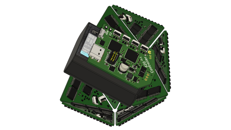
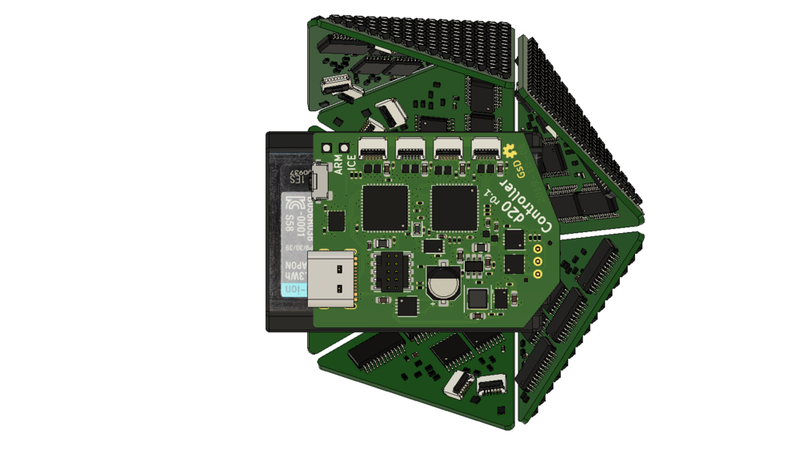
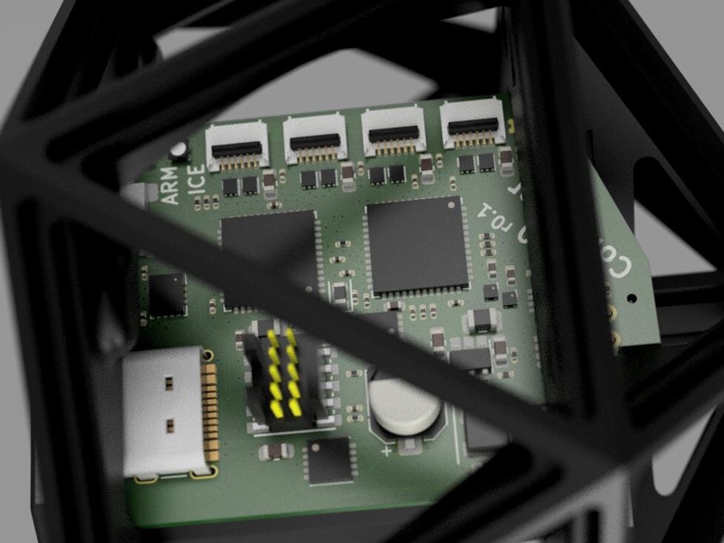
Controller
I’d re-designed the controller, basically an exact replica of the one used on the cube, but with 4x 6 pin FFC’s out to the displays. The controller and enclosure were designed in tandem, there was a bit of back and forth to get everything to fit correctly. Thankfully this is pretty seamless with the dxf import in KiCad and the 3d STEP output.
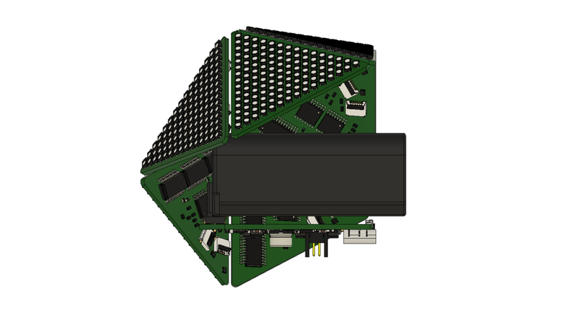
The controller is based around a fast programmable SAMD51, this is an M4 core that can run up to 120MHz. Also, because the project wasn’t complex enough I decided I’d like to use rust to drive the system. And there are rust crates and support packages for the samd51.
A button and USB connection ensure an easy way to update the firmware on the device, since access to the JTAG connector will be tricky once everything is assembled.
The ice40 FPGA offloads all the real-time display multiplexing, it outputs pixels to the 4 strings of panels in parallel, and achieves ~100Hz update rate from the frame buffer, while outputting gamma corrected 10 bit binary coded modulation for grayscale control over each pixel.
On the power supply front, it would have been nice to have a battery charger, but these Sony batteries are 7.4V nominal, which makes charging a tad more complex than just dropping in a single chip solution. I did still want tho device powered over USB when programming/debugging, so I added an ideal diode controller, which efficiently combines two input power sources. I also added a basic under voltage monitor to the battery to ensure that I didn’t over discharge the LiPo cells (Although I’ve now discovered that they might have this built in.)
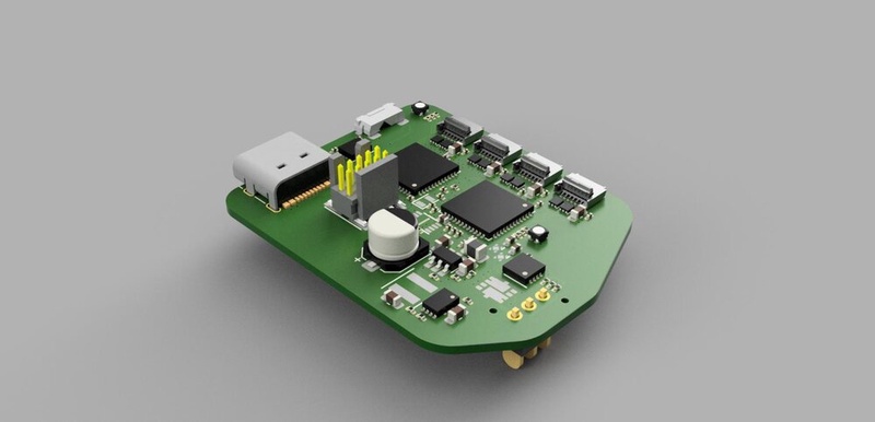
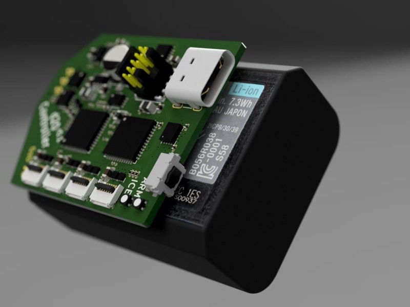
This is the model I’d created for the controller. This is straight out of KiCad, and was essential to ensure a good mechanical compatibility between the PCBA’s and enclosure.
I ordered these on the 10th October.
Assembly Stage
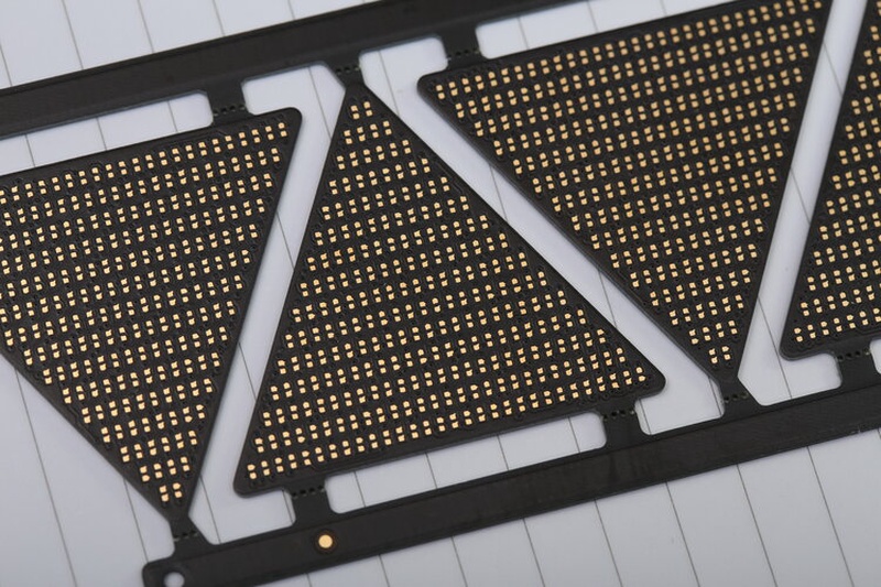
Circuit boards arrived on Friday 18th Oct.
Rapidly running out of time, I know I wanted to get a controller built, so I could start playing with the firmware. Also some LED panels built, so I could do a test-fit on the enclosure that would show up the following week. I got into a rhythm and ended up assembling the controller side on all the LED panels.
The soldering went great. I am using SAC305 Pb free paste, and stainless steel stencils that JLC provided with the PCBs.
With the controller side done I set up a jig to align the stencil on the top layer and apply solderpaste. I opted to do the LED side last mostly so that the LEDs only had to run through a single reflow cycle. I made a jig out of old PCBs to hold the panels by their rails in the oven, so that underside components were not touching anything. Surface tension should keep them all in place, but if a force was applied while the solder is molten there is a chance that they would move.
With solder applied to the PCB I placed the parts using a syringe with a blunt / bent dispensing needle. The syringe is connected to a small DC vacuum pump. This creates enough pressure to pick up parts from tape, and then when placed onto the solderpaste the extra force from the paste is enough to pull them off the syringe.
I set up a wooden board on my table and used double-sided tape to stick down strips of the LED cut-tape, all in the same orientation. The PCB is positioned such that the LEDs just have to be moved, not rotated.
I also built up a controller PCB. Also using solderpaste + reflow oven. And the enclosure arrived!
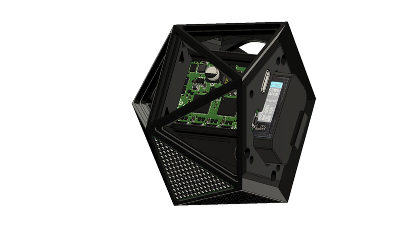
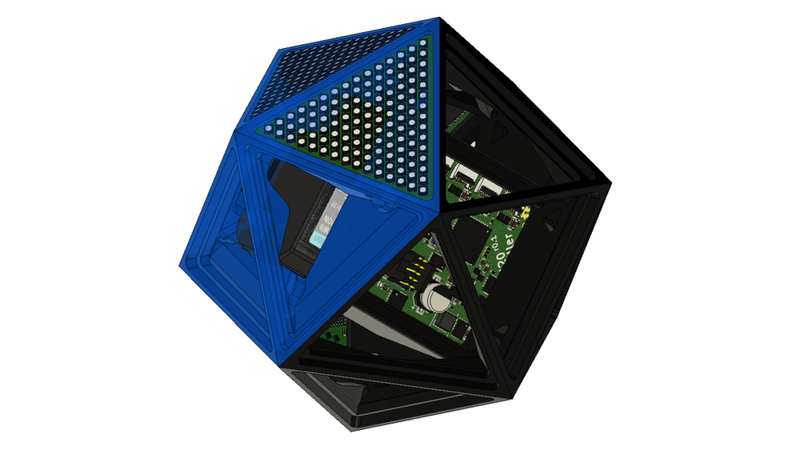
Enclosure Test-fit
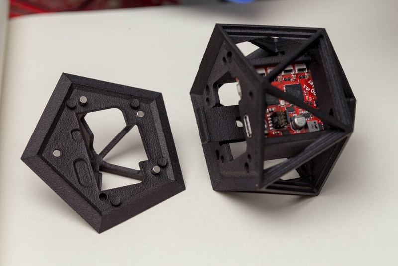
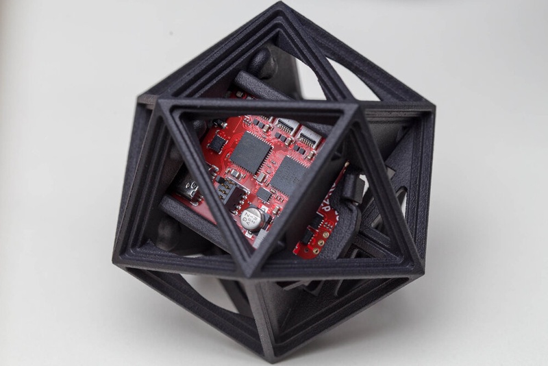
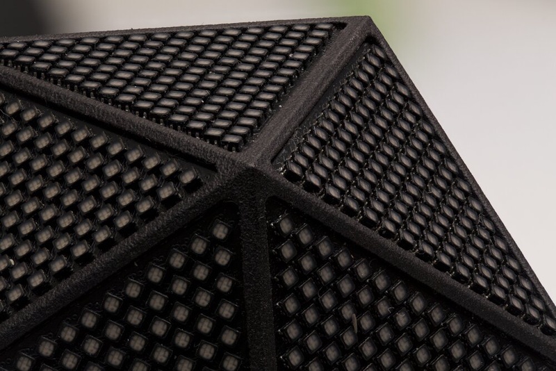
The enclosure looked great! The texture from the MJF was a perfect fit with the look of the PCB/LEDs. The tolerance between the parts I had estimated perfectly. The magnets fit in both parts (One problem was I couldn’t actually get the magnets out.)
The controller board and battery fit great in the enclosure. So now it was time to dive into the firmware/gateware and get the LED displays working.
Firmware and Mistakes
I’d been putting this step off for a little while, because the gateware needed to be altered from the cube in order to drive this new panel type. The row and column data needed to be encoded into a 64bit pattern and then sent out to each display in the string.
I coded this change up in a simulator, and confirmed that I was getting the correct signals out. So I hooked it up to an icebreaker (ice40 development board) and run my gateware. Nothing.
…
Nothing happened.
This is not really unsurprising to be honest. There are a lot of things that need to be set correctly in order for code that looks correct in a verilog simulator to run correctly on hardware. So I powered up my scope and began probing around.
- Signals coming out of the FPGA: OK
- Signals appearing on the shift register inputs: OK
- Blank signal toggling: OK
- Latch signal: OK
- Data coming out of shift registers: OK
- Voltages: OK
- LEDs turned on: NAK
Eventually I tested the value into the PMOS switches. Hmm, that’s weird. There was a signal on it’s gate, as expected, but source isn’t changing. Did I get the footprint wrong?
I took off all the PMOS high side drivers on one of the boards, and bridged gate to drain. So effectively the 74 series 595’s were driving the LED high side directly.
Big Ooof. -______________________-
Current Date 20th Oct
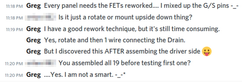
I had use the wrong footprint on both the r0.1 boards that had an incorrect LED footprint, and then also again on these! And didn’t pick up on it until now. So with less than 2 weeks I may have had just enough time to order new boards with this fixed. But then all 20 of the boards I’d built would be scrap.
Bodge time
The temporary fix I’d put in place on the first board wasn’t going to work. The 595’s do not have enough current driving capability to match the current sink drivers. So when more than 3-4 LEDs are lit a single row the brightness really starts to dip, this produces very undesirable effects for the way the display is wired up.
Just a few rework items how bad can it be?
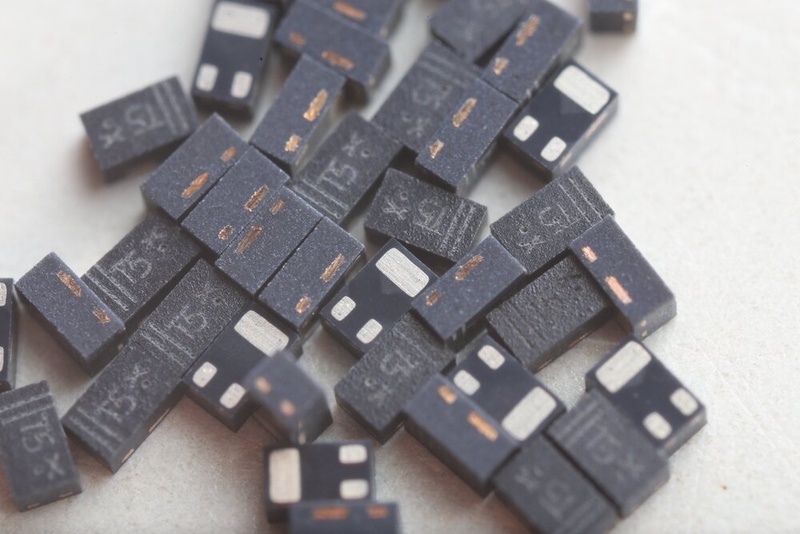
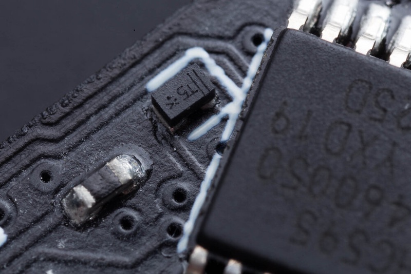
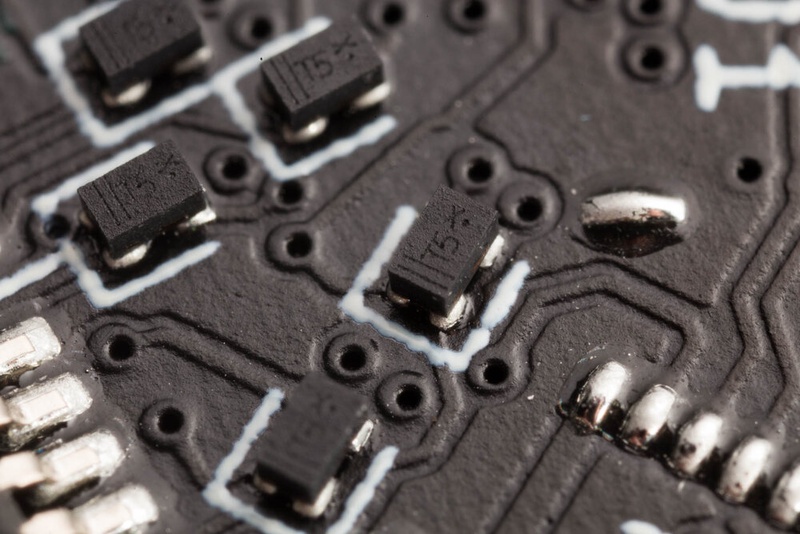
The mosfets are in SOT-883 packages, which is the same size as a 0402 resistor. They have 3 pads underneath.
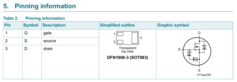
As shown in this datasheet page for an equivalent part.
Note I did try and find a part with different pinout that would match my PCB. Unfortunately for me manufactures often like to stick to industry standard pinouts, so they can be drop-in replacements for competitors. It doesn’t really make any sense to release a mosfet with a different unique footprint.
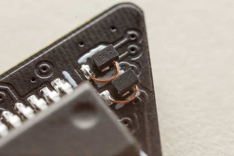
My issue was that I had swapped G/S, the two smallest pads. My plan to rework these was to rotate the part such that the G/S pads were in correct orientation. Then with a small length of magnet wire connect the, now displaced, drain back to the PCB.


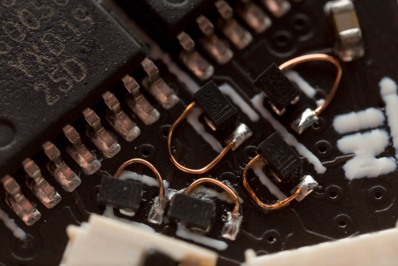
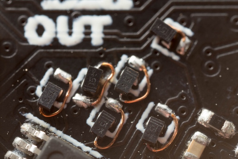
So that’s exactly what I did. For every PMOS on the LED panels.
Let’s do some math real quick. 15 PMOS per panel * 20 panels = 300 bodge wires.
So that’s why I started using the saying “This project has 300 bodge wires inside”. I’m not sure on exactly how long it took me to complete all the rework, but I did make it through a 60Hr Audio book that week.
I tried to have a bit of fun and film some rework under a thermal camera. This is a Boson 640, running at 30Hz with the widest lens. You can see a bit of distortion effects from the lens.
Wrapup
I worked through each panel in turn, and did in fact manage to have it all completed (and working) before departing to the US on 2nd November. I did get quiet a few interesting questions from friendly folks at security. I think I generally I would describe it as an electronic art project.
Here is a short video timelapse of the device being disassembled, assembly is the process just in reverse.
Here is what one of the basic animations looks like.
Overall I’m very happy with how it turned out, and I got lots of positive feedback on the project at supercon.
Downloads
If you’re feeling adventurous and want to build one of these for yourself I’d love to see it! Alternatively you can just check out the design files.
Here is a repo with 3d printable files, and hardware designs for PCBs: https://github.com/gregdavill/d20-hardware
The proof of concept firmware that’s running on the device was written in rust, and is available here. (currently embedded in a modified atsamd crate that I added DMA support to): https://github.com/gregdavill/atsamd/tree/d20-controller
Gateware for the ice40 is based of the rgb_panel code from Sylvian “tnt” Munant, but with a slightly modified “phy” to support the unique shift register design of my panels: https://github.com/gregdavill/ice40-playground
Future work
The controller is a big aspect which could be improved. Adding something with wireless connectivity would be great, to be able to sync up patterns and animations with another device.
The panels are working great, and r0.3 updates them, so they don’t require the bodges.
I think a new controller board might include either an ESP32 or ESP32-S2 chip, along with the FPGA. This would provide a nice way to add extra features, while not having to worry about the tight timing on the display side of things.
Mapping of the pixels into a coordinate space would be very useful. I think this probably isn’t actually too difficult, but just requires wrapping my head around matrix multiplications to move the grid of pixels on each face from a 2d plane into position in 3d space around the icosahedron, then each pixels’ location can be recorded and used in a lookup table fashion to create interesting animations and effects. Charlie and his new favorite toy