I’d recently bought a new XPS13 7390 (non 2-in-1) laptop. I had bought the 8GB variant, how hard could it be to upgrade?
I use my laptop for KiCad PCB design, compiling embedded firmware, and FPGA synthesis. None of these really use that much RAM. But if you leave tabs open in Firefox or Chrome and also perform other work you’re easily going to exceed 8GB. I’ve done so many times, on my ubuntu install the system basically grinds to a halt as the kernel scrambles to unload pages from DRAM into SWAP.
I knew the DRAM in my new laptop was soldered to the main board when I bought it. But I’m an electronics engineer, and reasonably proficient at BGA rework. So this begs the question, How hard is to actually upgrade?
Initial Research (asking on twitter)
I had my old laptop, an XPS13 9350 that contained 16GB of LPDDR3, contained in 4 separate ICs. This means that each IC contained 4GB, (or 32Gbit). I was curious about performing a direct swap from the old system to the new one.
I posed the question on twitter.
I’m curious about upgrading the DRAM on my new XPS. 8CB -> 16GB.
I have my older XPS MB with perfectly good LPDDR3 chips, I’m confident I could do the rework to transplant them.
Would the BIOS just pickup on the extra RAM? or is there other SW steps involved?
I honestly didn’t expect much from this tweet, but whitequark replied with a concrete answer!
which exact models? on 9350/9360 there are hard straps. I suspect it will be the same on newer but I’d need to check schematics to be sure.
Not only was this super helpful, she went multiple steps further! locating a schematic and board view for my laptop, to verify these resistor straps.
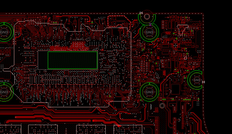
With the board view I was able to locate the resistor strap on my mainboard
There was also a hackaday.io project I found of someone doing the same procedure but on their MB pro.
How socketed RAM works
If you’ve ever taken a close look at a SODIMM that you might use in a laptop with “user upgradable” memory. There are the RAM ICs, plus an extra small IC, typically a 8-pin TSSOP part. This is known as the SPD, Serial Prescence Detect. Essentially the RAM ICs on a SODIMM are just that, RAM. They don’t contain any method or mechanism to query what capacity/speed they are. So instead of performing an exhaustive self-test over the entire memory array to detect what RAM is installed in a system, SPD was created. It’s essentially just a small EEPROM that describes the ICs that are installed on a given SODIMM.
When laptops started moving memory onto the mainboard, instead of in sockets, they still needed a mechanism to emulate SPD info, so that your OS can correctly detect and show you information about the memory installed in your system. Instead of populating an EEPROM, they simply embed this info inside the BIOS FLASH. Part of the BIOS boot sequence is to extract an SPD table from FLASH, and create a virtual SPD that the OS can query.
How does this help us
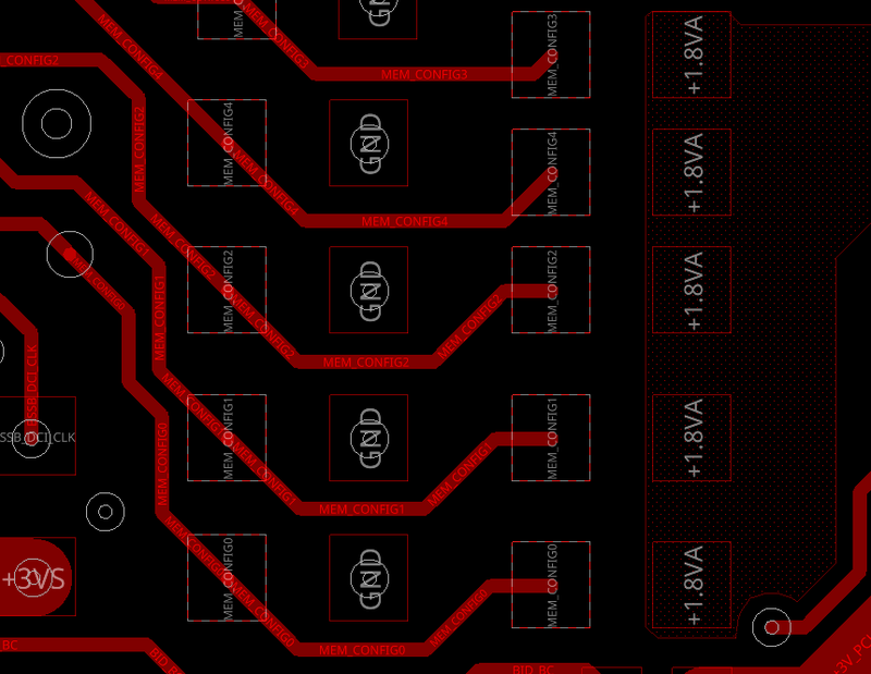
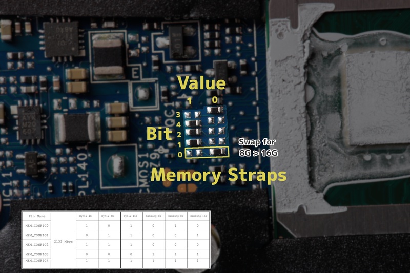
Knowing that there was a 16GB model of my laptop available to buy helps here. Dell release the same BIOS update for the XPS no matter what RAM is installed, so they use resistor straps on GPIO pins of the CPU to detect various mainboard variants. These values are published right in the schematics
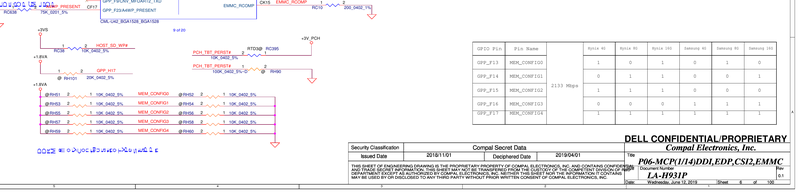
You can see here a series of 5 “strap” resistors, and a table which shows that they can be populated in various arrangements. Note: the table specifies specifically 2133Mbps, and shows values for Hynix, and Samsung parts in 4/8/16G variants.
Great! I suppose the next step will be to jump onto a component distributors website and buy some new ICs right?
Buying new chips
As it turns out, LPDDR3 memory isn’t really stocked through standard distributors. Digikey only had a fow listings for lower density parts, at slower speeds. To source these parts I might have to get creative.
What got me started on this idea was that both my old XPS13 (9350) and the new one (7390) both use LPDDR3. Would it be possible to list the parts from the old mainboard and install them on the new one? Well, probably not. Remember how I mentioned that the schematic specified 2133Mbps? Well the LPDDR3 from my old mainboard was only rated at 1866Mbps.
Whitequark pointed out that there are some other dell laptops which use the same 5 resistors straps, and show a larger table of memory options. Maybe they left the extra SPD tables in the BIOS? I think I had certainly nerd-snipped her at this point, because she went as far as decompiling the BIOS and extracting part numbers of all possible strap configurations, and deemed that only the values shown on the schematic were present.
So looks like I will need to find some 32Gbit 2133Mbps ICs. It’s possible to pick up mainboards from ebay that would have the parts. But that can get to be a bit expensive, especially since many laptop mainboards also contain a soldered down CPU.
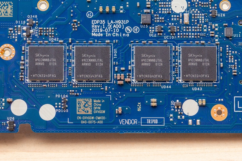
So I went to aliexpress, typed in a part number that was extracted from the BIOS’s SPD data; H9CCNNNCLGALAR-NVD and would you look at that.

I bought exactly 4, 2x “New Original 2pcs”. I placed an order on Jan 2nd 2021 from this listing.
Reliable+Professional=We? Yes, Indeed!
Now the fun begins
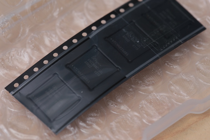
Feb 19th 2021: A package arrives. They do in fact look “New Original”!
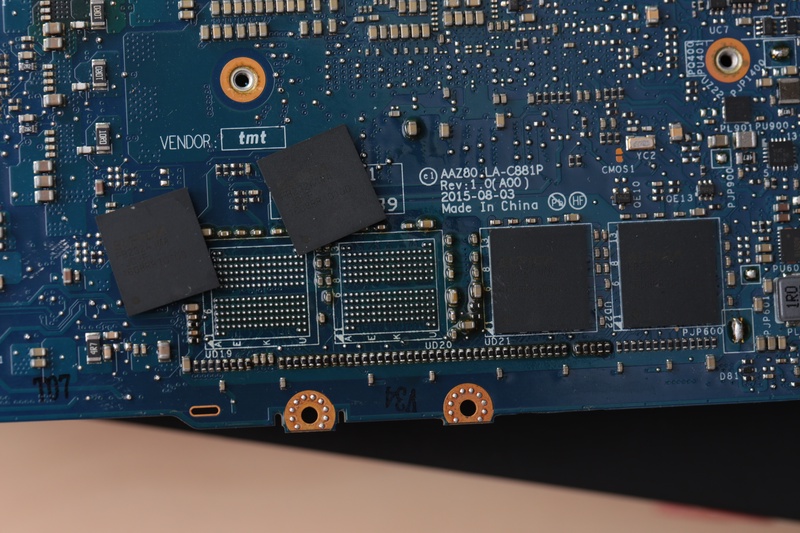
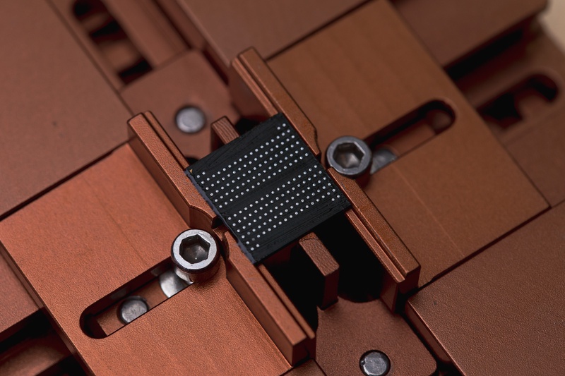
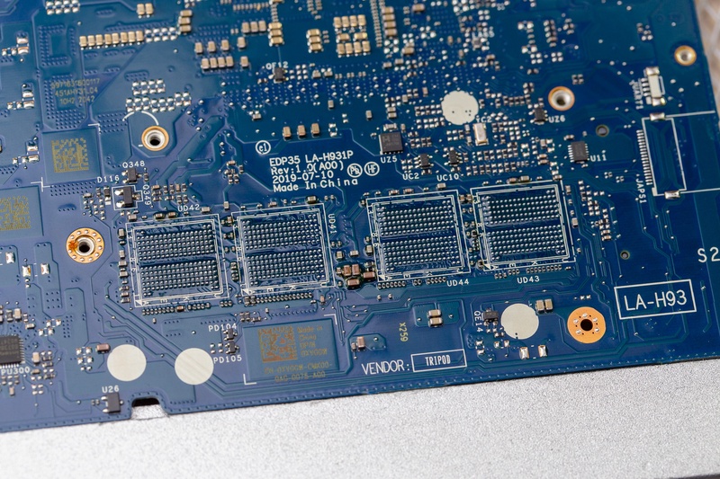
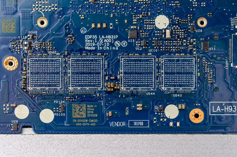
Having checked out the boardview for the motherboard I now know it’s an 8L design with 3/4 ground-planes throughout. So quite challenging on the rework side. Not wanting to ruin a perfectly functional laptop, I decided to practice on my older laptop main board first.
Using my hot-air gun a Quick 861DW, and a no-brand pre-heater under the PCB I started to remove these old LPDDR3 parts. It was a good thing I practiced, because to overcome the multiple ground planes you really do need to pump a lot of heat into the PCB before the lead-free solder begins to melt.
Are the new parts even genuine?
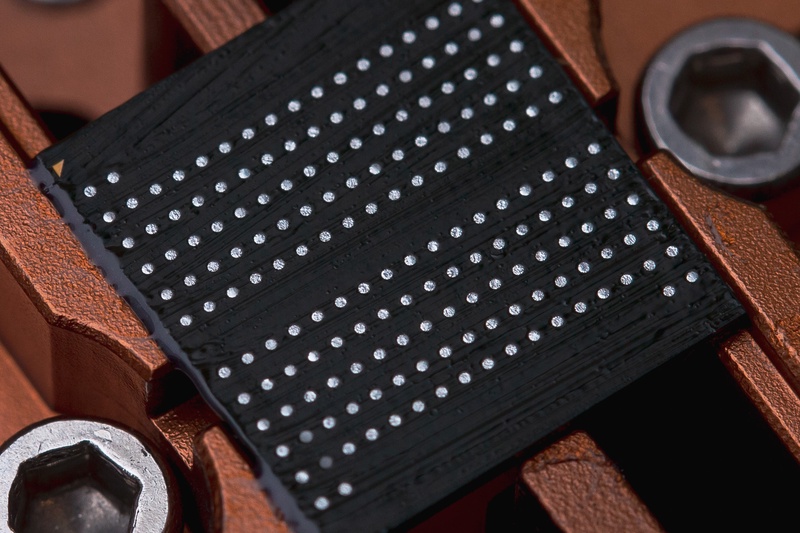
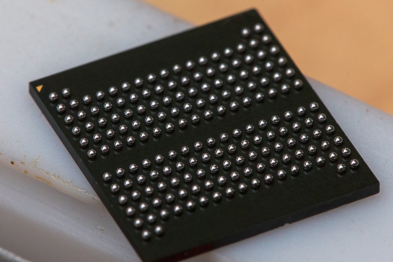
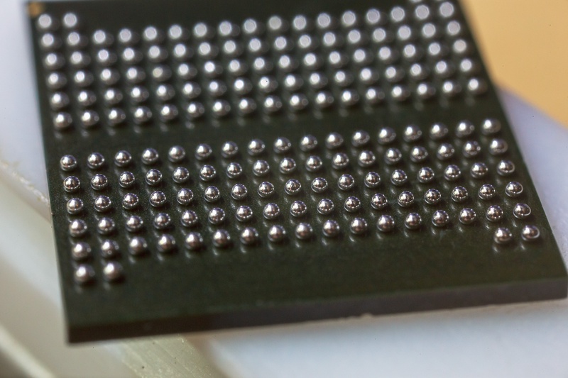
Even though they weren’t super cheap, I wasn’t sure if they were actually genuine or not. The first check was that yes in-fact the ball pattern matched LPDDR3. My second check, I used a bit of acetone on a cotton swap to rub the top of the IC, if the IC were cheaply re-marked with paint/laser then this might reveal a fake. No paint came off with the acetone.
Lastly, and this is definitely overkill. I had a dentist take an xray of the new and old parts.
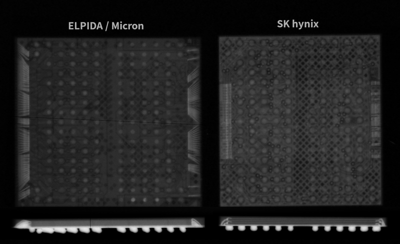
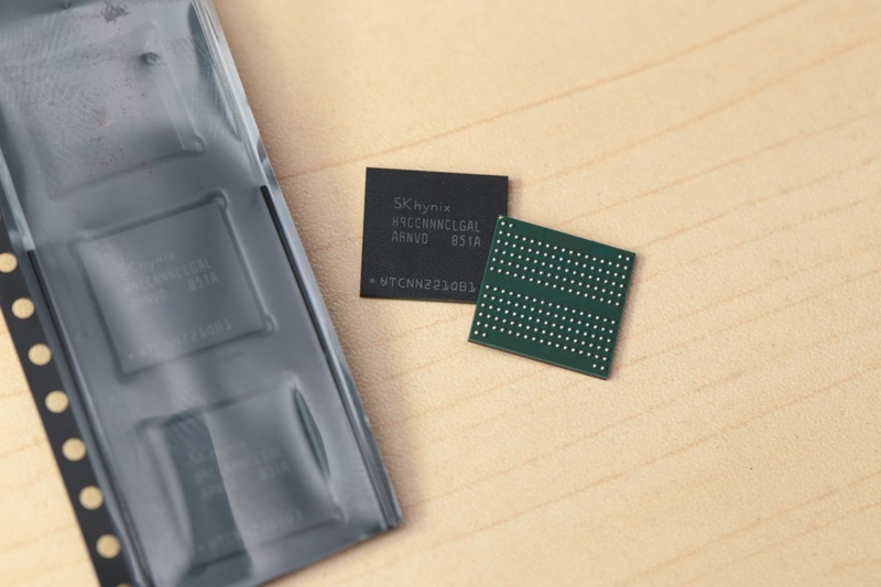
So clearly what I had was a DRAM part, you can see a die inside there and also the bond-wires running up to the dies from the substrate. What’s fascinating to me is the fact that you can clearly see this is a multi-stacked die, one way they’re able to fit 32Gbit inside a single chip. And the fact that the new/faster SK Hynix parts are making use of a considerably smaller die! It only takes up half the total package, compared to the older LPDDR3 where the dies is the majority of the package.
So even after the xray I’m still left without an answer. But I can really only assume that it is a genuine part, and solder it down.
Soldering BGA parts
De-soldering BGA parts is pretty straight-forward; Apply heat, when solder melts lift up IC. Of course there is a fair amount of skill involved, practice helps!
Once you’ve removed a BGA part, some solder is left on the PCB. But some remains on the part. This doesn’t happen evenly across a part. So if you attempt to solder that part back down to a different PCB then some connections may have too much solder, and others not enough.
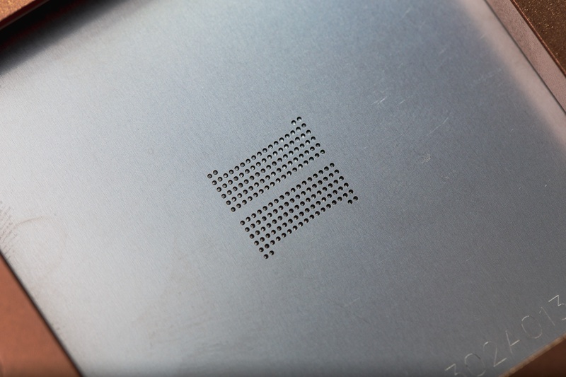
If you wish to re-populate a BGA part that you’ve removed you really do need to perform “BGA re-balling”. I wanted to practice this, so I bought a BGA re-balling kit, and a stencil for the LPDDR3 parts.
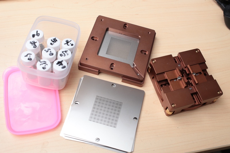
The first step is to remove all the existing solder from the IC, and clean off all residue and flux.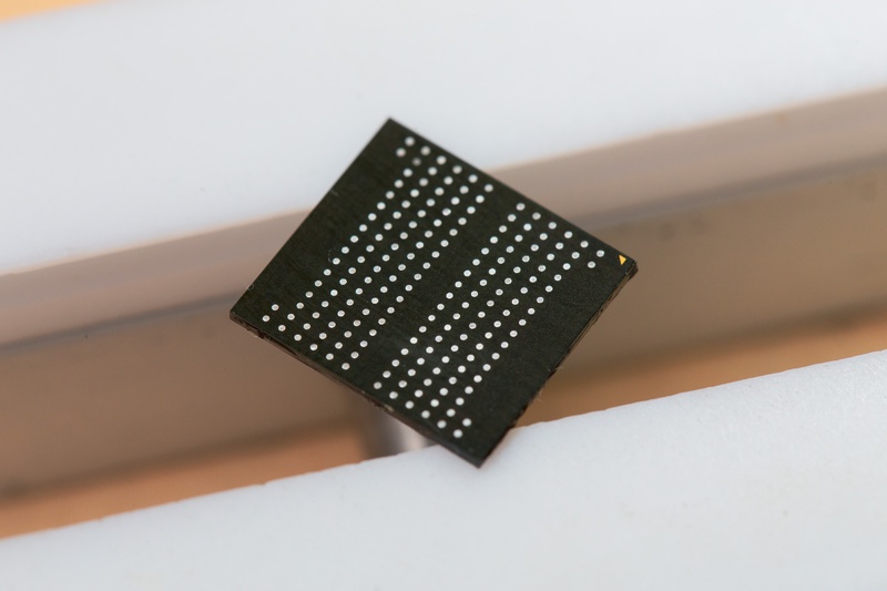
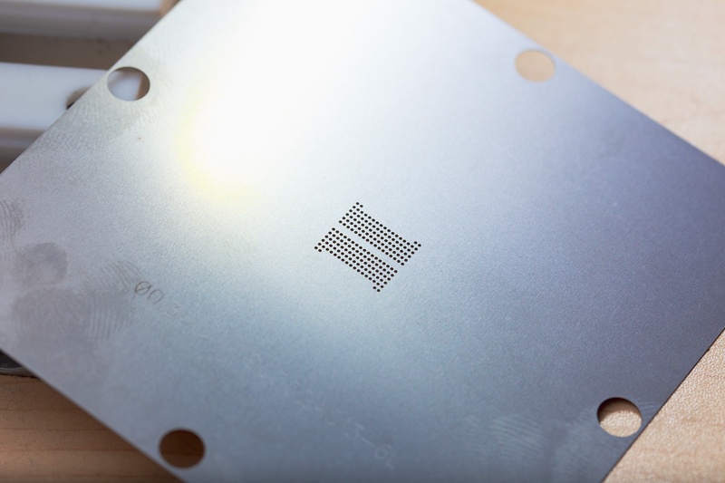
With the part loaded into the jig, a thin layer of flux is applied to the IC, and the stencil is aligned
Solder balls are added to the jig, and spread over the openings in the stencil.
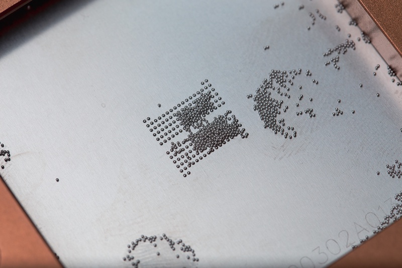
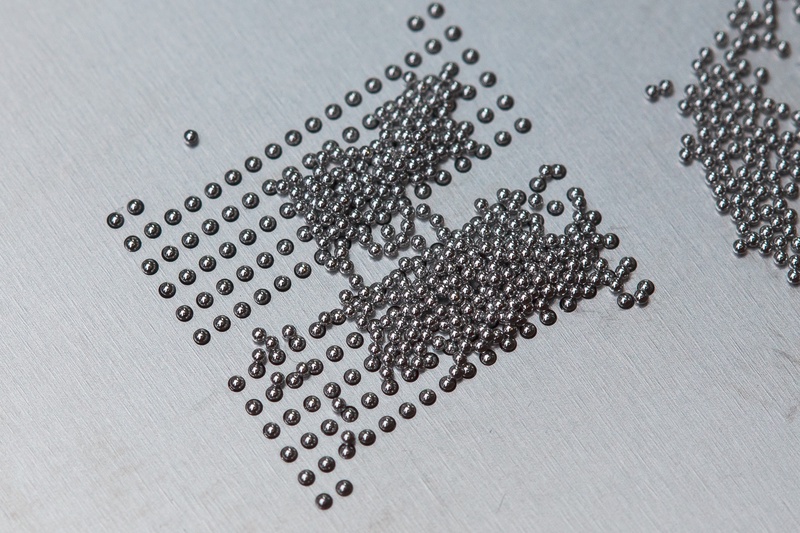
After clearing balls from the openings you can lift the stencil up
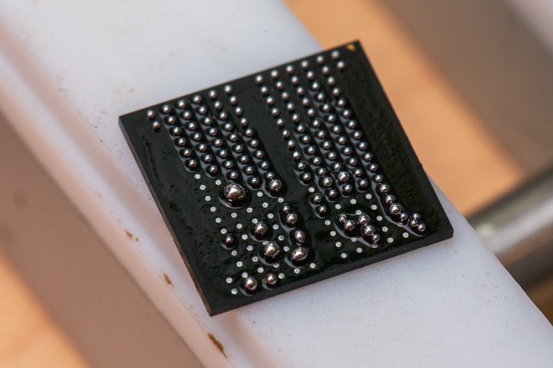
Note that you could see the balls weren’t perfectly aligned in the last image, and this resulted in a pretty bad time. No worries, just return to step 1 and start again.
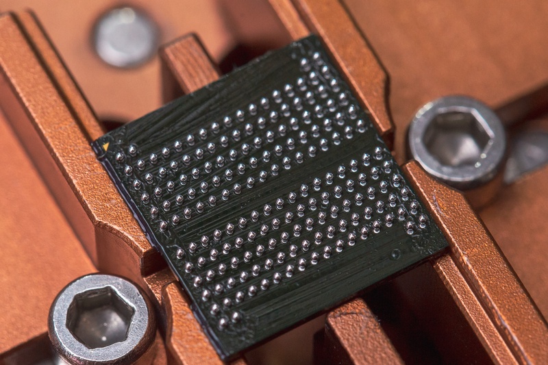
If you get everything right you can have a perfect looking part, read to be soldered down
I got pretty confident in my re-balling, and actually re-balled all of the new LPDDR parts. This removed the lead-free solderballs and replaced them with leaded solder. My lab is generally a lead-free space. However in this case the lower melting point would help my chances of success with soldering down the new ICs.
Upgrading the RAM
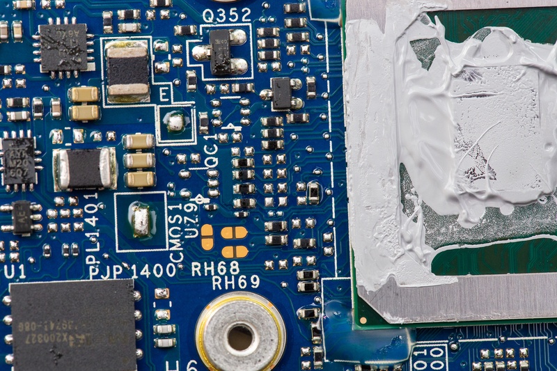
With enough practice to be confident in my abilities, I created this little graphic, showing the exact resistor I needed to move. Nothing else to do but to actually swap the RAM chips.
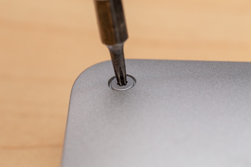
The XPS13 comes apart pretty easily with only a few external torx screws, then phillips screws throughout the inside of the machine
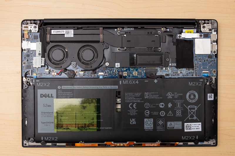

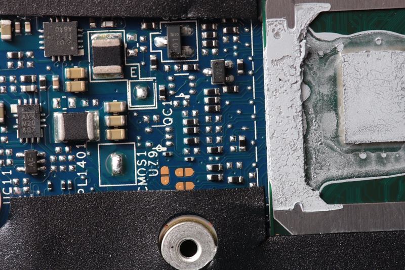
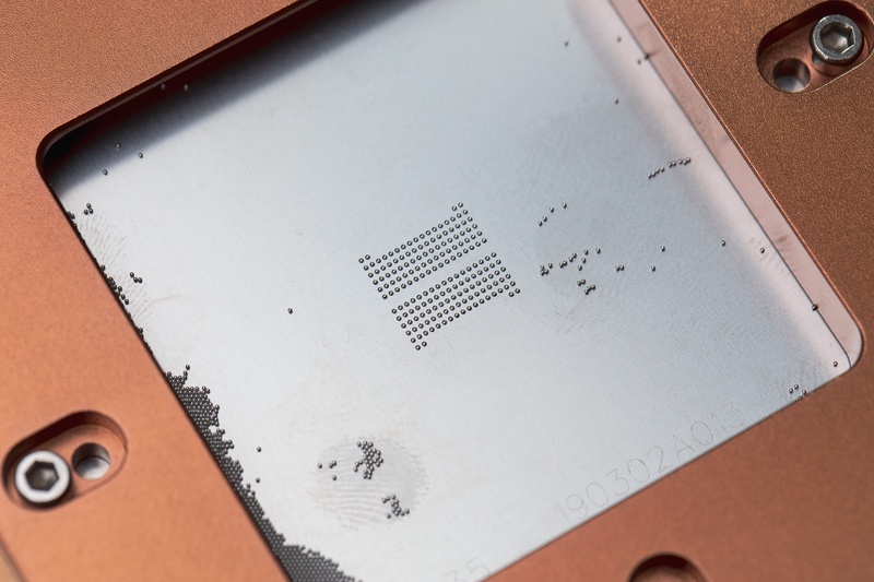
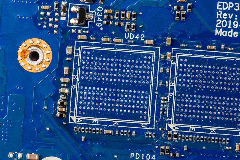
Here is the installed LPDDR3 parts, these need to be removed.
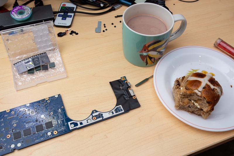
But first a quick break to refuel. With a hot Milo, and hot cross bun. Yumm.
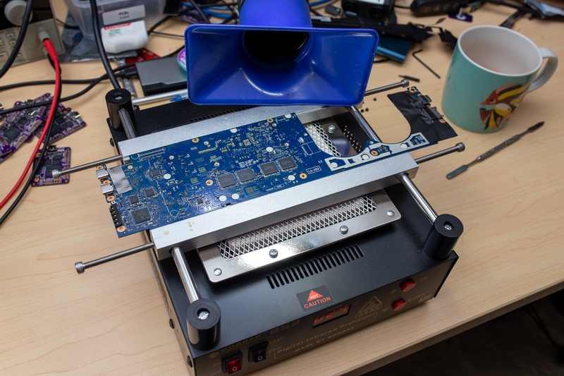
Here is my setup, IR pre-heater, main-board, and fume-extractor. Not pictured is a stereo microscope above this stack.
With all my practice the RAM came off without an issue
After the ICs were removed I used solder wick to remove any excess solder, then cleaned up the area with IPA.
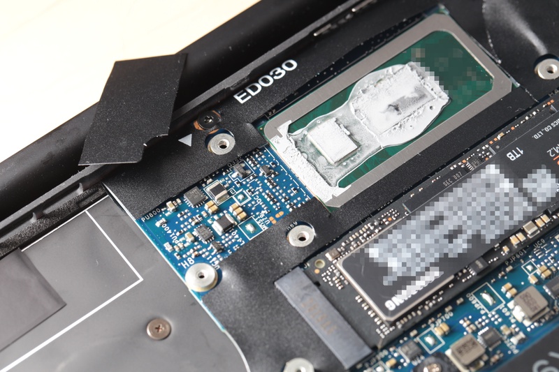
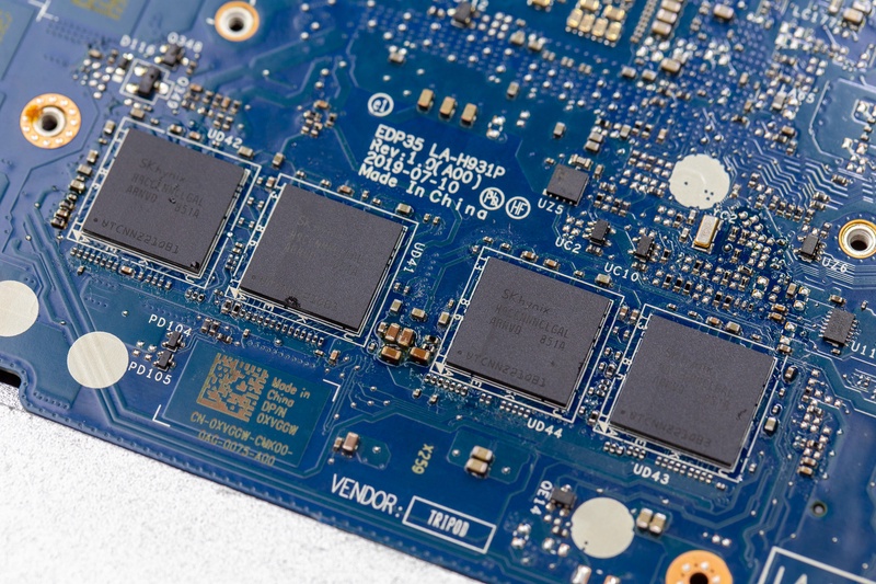
New RAM installed
And strap resistor moved, so hopefully the BIOS will know there is 16G present.
Is that it?
A small strike of panic as I pressed the power button for the first time after putting most of the machine back together. In order to work on the main-board I had removed the CMOS battery. Turns out the XPS will take a solid 30-60s to boot up after the CMOS battery has been removed and replaced.
Phew.
Back into the BIOS and look! It’s detected it!
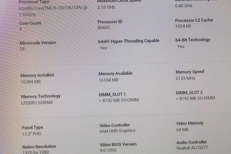
But this is probably expected, simply due to the straps. The BIOS doesn’t actually run any memory checks. So likely you could get this result even if the 8GB was still installed.
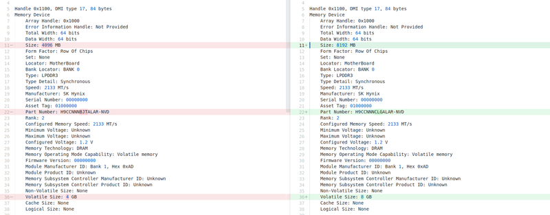
Exiting the BIOS the computer booted normally in to the OS. This is a good sign. It’s unlikely that an OS could boot if the reported RAM didn’t actually all work. I ran a quick check from the OS on the SPD. Which looks good, mimics what we saw in the BIOS.
Final Testing
With an OS booted I was pretty sure that the ICs were in fact genuine. But to ensure system stability, and to ensure that I’d actually soldered them down correctly you do want to perform an exhaustive memory test. So as a final step I fired up memtest86. and let it run through.
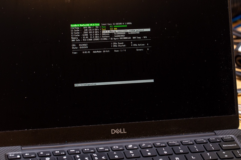
It passed through 4 passes of all its tests without issue! This shows that all the memory space is functioning and my RAM upgrade was a success!
Conclusion
I’ve now got an XPS13 with 16GB of memory.
But next time I think I’ll just buy the 16GB variant upfront.