Background
Having seen a few projects creating LED cubes from panels used for LED video-walls I knew I had to try to build one myself. If you haven’t seen these before here are some examples I’ve seen. along with some notable people involved in their creation: @zzaurak, @1HappyTeddybear, @esden, @kernlbob.
These cubes are all built using COTS video wall panels. The mains ones I’ve seen used are in the 64x64 pixel size and either 2.5mm (P2.5) or 2mm (P2) pixel pitch. These panels feature a low cost multiplexing system on the back of the PCB, and a dense array of LEDs on the front. Surprisingly these panels are made surprisingly cheap, with panels from China costing $20-$40 range, which for 4096 RGB LEDs is very cheap!
Of course I had to buy some of these panels to play around with.
These panels typically arranged as a top half and bottom half. The multiplexing arrangements means there is 2 lines lit at any one instant. And they feature a control interface known as HUB75. This interface consists of the following collections of signals:
1x 5bit bus that is used as a 1 to 32 decoder this activates a single row.
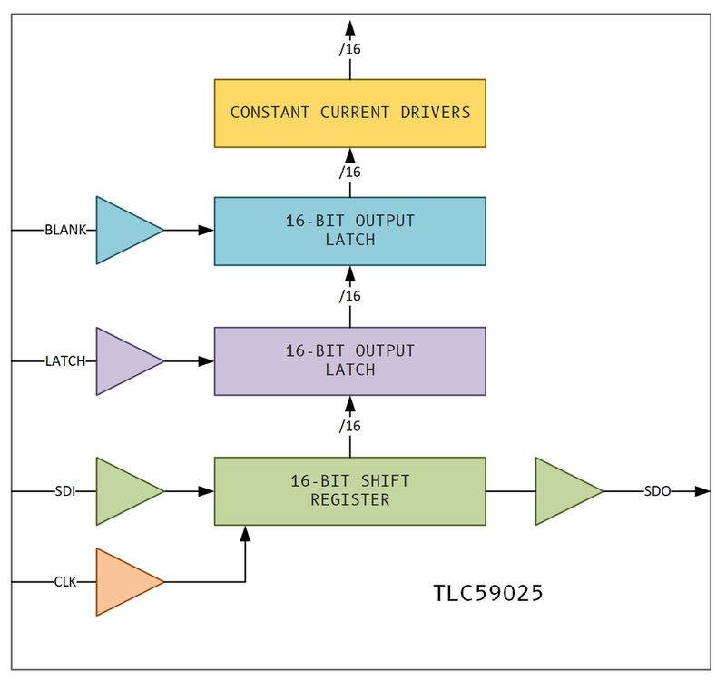
3x 2bit shift register inputs with common latch and blank signals, that is used to control data output to the column. There is one input for each colour [R,G,B] and then for the top/bottom of the display.
These panels are multiplexed, meaning that only a single line of data is displayed at a time. To further reduce hardware costs the driver circuitry can only turn each pixel on/off. No grey-scale control in the drivers. Because of this, in order to display an image over the entire screen we need to constantly update data on the panel line by line, and rely on an effect called persistence of vision for our brain to blend these scanning lines into a solid image. In order to display greyscale values we apply a second level of modulation on top of the traditional line scanning. This modulation know as Binary Coded Modulation, or BCM, allocates time slices doubling in length to each bit in our greyscale pixel values for R,G,B. Mike Harrision has made a very detailed and informative video on this topic: https://www.youtube.com/watch?v=6iHTbGsnI8Q
For all my experiments I’ve used the icebreaker FPGA board: https://github.com/icebreaker-fpga/icebreaker And RGB panel code that implements a frame buffer and the multiplexing+BCM from @tnt: https://github.com/smunaut/ice40-playground/tree/master/projects/rgb_panel
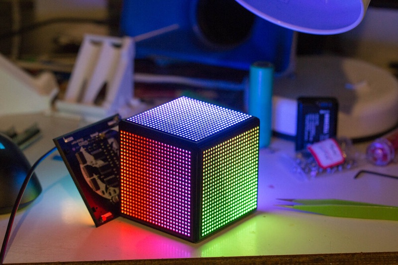
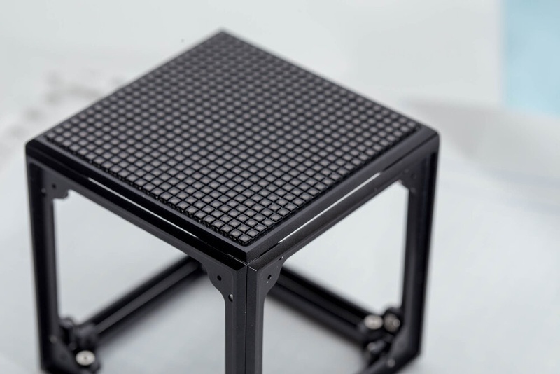
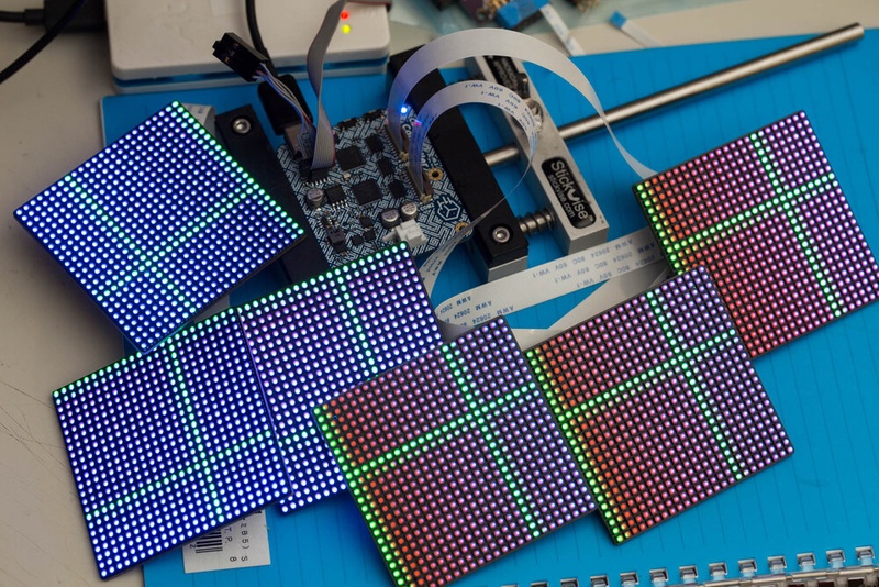
With some P2.5 panels in hand I poked around with the idea of making one of these full sized cubes
I wasn’t super pleased with the overall size of this, it was simply too big. But how could we make it any smaller? Sure the P2 panels are a bit smaller, but still make a cube in the 120mm³ size. To make one smaller would require designing and manufacturing a smaller LED panel…
Designing a smaller LED panel
So that is basically what I did. It turns out you can buy the LED used on these panels for very cheap from LCSC at around 2c per LED when you’re buying them in the 2000+ qty. (Full reels are 13,000 LEDs. and you can probably get them down to around 1c when buying multiple reels from Alibaba, or direct in Chinese markets) Additionally the shift registers used in the multiplexing control electronics are also very low cost. There is already some very useful information and documentation about existing LED panel designs: https://github.com/esden/led-panel-docs
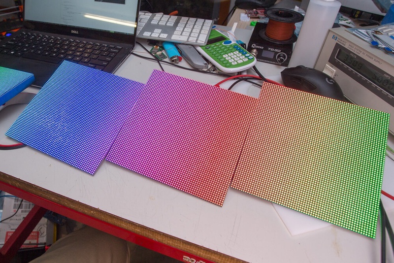
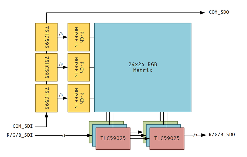
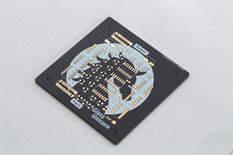
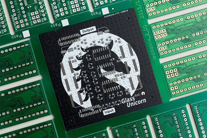
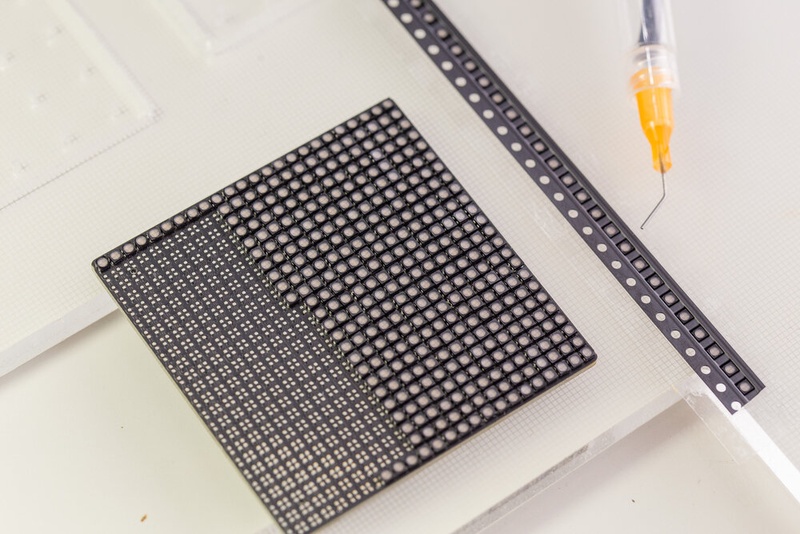
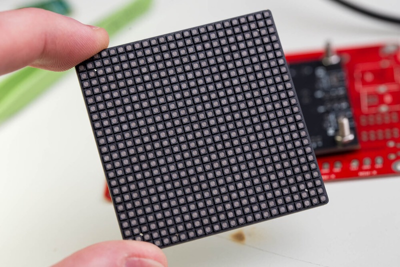
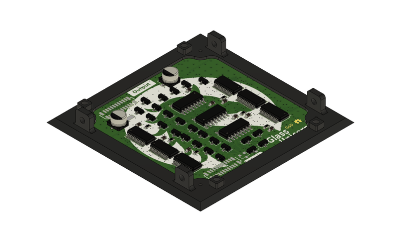
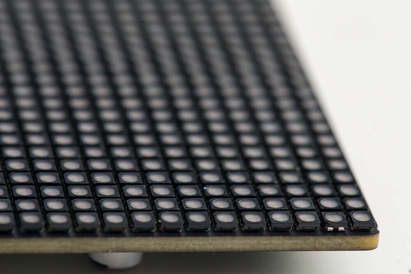
With a schematic of one of these larger panels in hand, I created a schematic for my own smaller 24x24 panel. The actual architectural design of this panel is a bit awkward, since there are 2 shift register chains for rows and columns, one 32bits in length, the other is only 24bits. That is handled in gateware, but is a bit awkward.
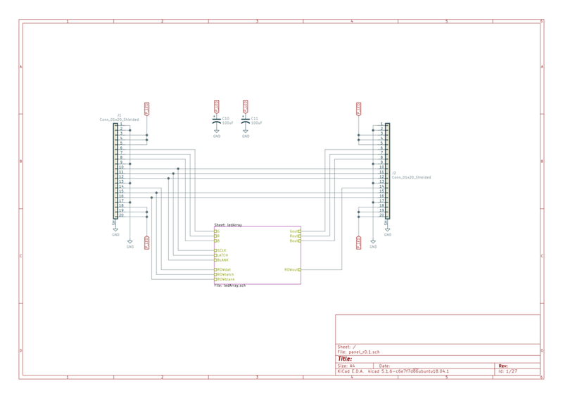
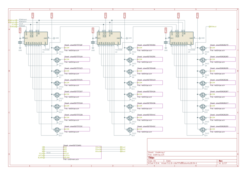
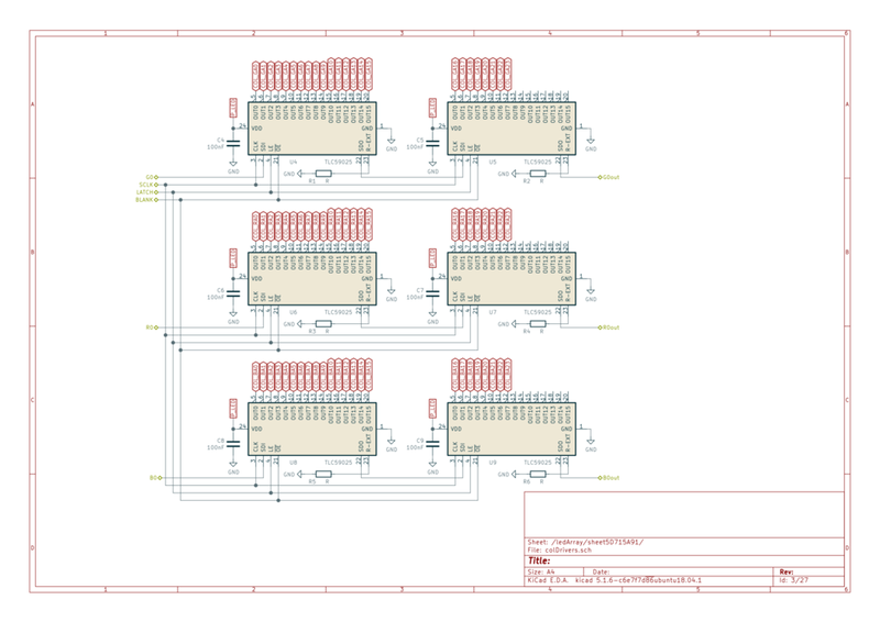
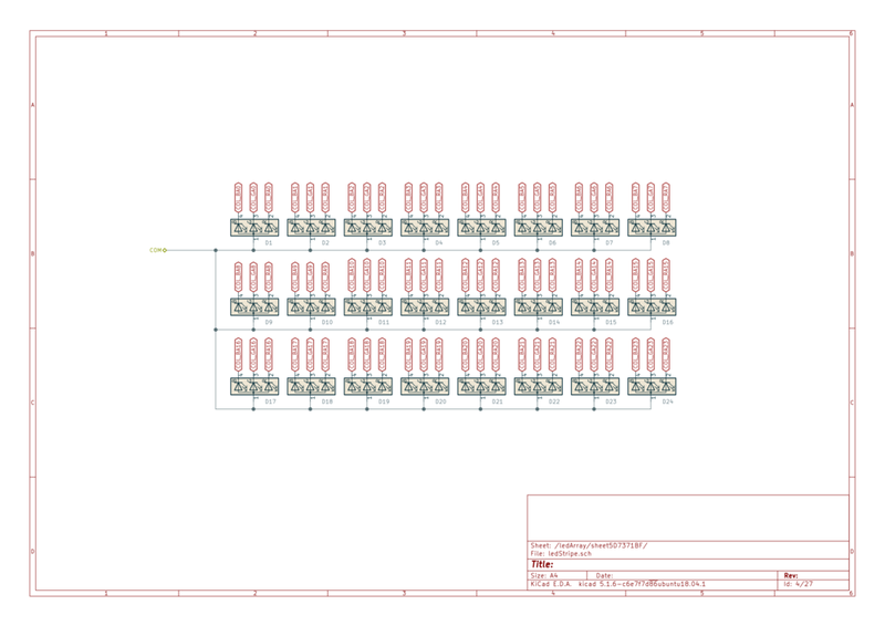
I tried to make use of hierarchical sheets in KiCad to ensure that the design remained somewhat reasonable. I think I managed a reasonable job, but there are still a lot of global labels around. It’s not easy neatly creating a schematic connection 576 LEDs.
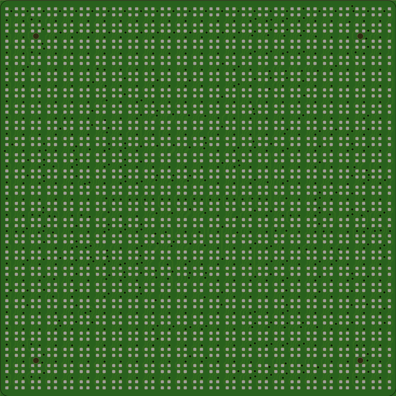
PCB layout was actually not too tricky and I even had a little fun with some artwork on the back.(Which you never see when it is fully assembled.)
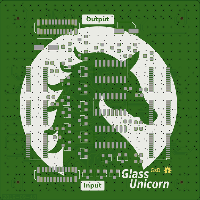
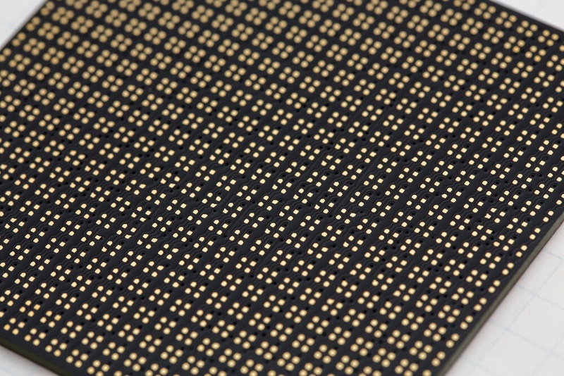
To ease routing I went with a 4 layer design. Every LED on the top has signals routed through for all the common R,G,B signals, these are for the columns and run downwards. Every LED has a common connection which requires a via and connection on layer 2 connection every row together. Because we want to use a cheap PCB manufacturer, and avoid micro/blind vias, we need to arrange the routing on the top layer to give room for an additional via next to every LED, we’ll use this to route signals from our controllers to the matrix, and also route signals required for the controllers around on layers 3-4.
It was quite an interesting routing challenge, but with some careful planning and heavy use of the array tool it’s not too difficult.
One thing that was essential was scripting in Kicad to move every led into its correct matrix position. This was achieved using the internal pythin scripting in KiCad and the following script: https://github.com/gregdavill/GlassUnicorn/blob/master/ref/led_32x32_array_place.py
# To run, open the KiCad scripting console and type: exec(open('../../ref/led_32x32_array_place.py').read())
#
# This script will re-position D[1-1024] into a matrix filling the specified width and height, at the location provided below.
# After running you will have to press F11/F12 to force the screen to re-render.

import sys
from pcbnew import *
pcb = GetBoard()

initialX = FromMM(120.75)
initialY = FromMM(70.75)
width = FromMM(61)
height = FromMM(61)
padding = FromMM(1.1)

count = 32
spacingX = (width - (padding*2)) / (count - 1)
spacingY = (height - (padding*2)) / (count - 1)
print(f'Spacing X,Y = ')

nCount = 1

print('Start Place')
for y in range(count):
    for x in range(count):
        Ref = f'D'
        nCount = nCount + 1
        #print(Ref)
        try:
            nPart = pcb.FindModuleByReference(Ref)
            nPart.SetPosition(wxPoint(initialX + padding + (x*spacingX), (initialY + padding + y*spacingY)))  # Update XY
        except:
            pass

print('Finished Place')
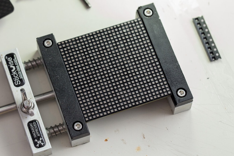
Assembly (Hand placing thousands of LEDs)
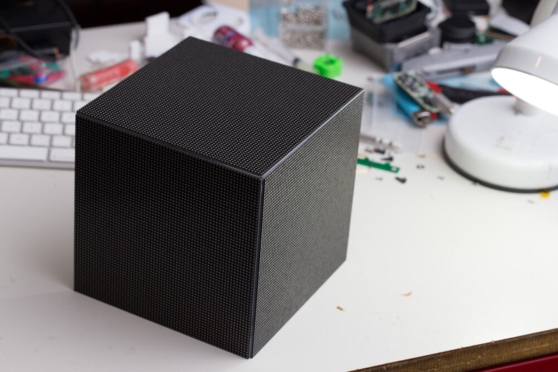
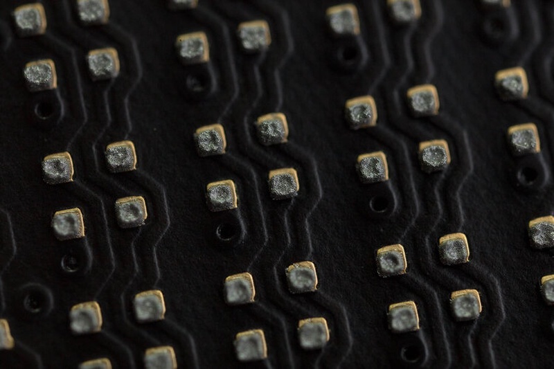
I had JLC sponsor the panel PCBs used in this project. So check them out if you’re after prototype PCB. I got the boards made in matte black with ENIG. Black PCBs really help on the LED side to hide the gaps between the pixels. ENIG provides a flat solderable plating to the pads making solderpaste and reflow soldering a little bit easier compared to HASL plating which sometimes results in SMD pads having a small ‘pillow’ of solder. Also in my opinion ENIG alss just looks better.
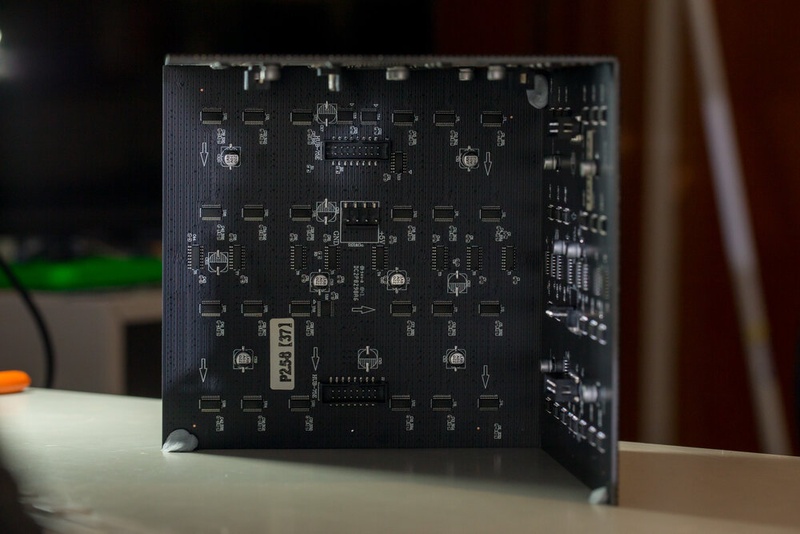
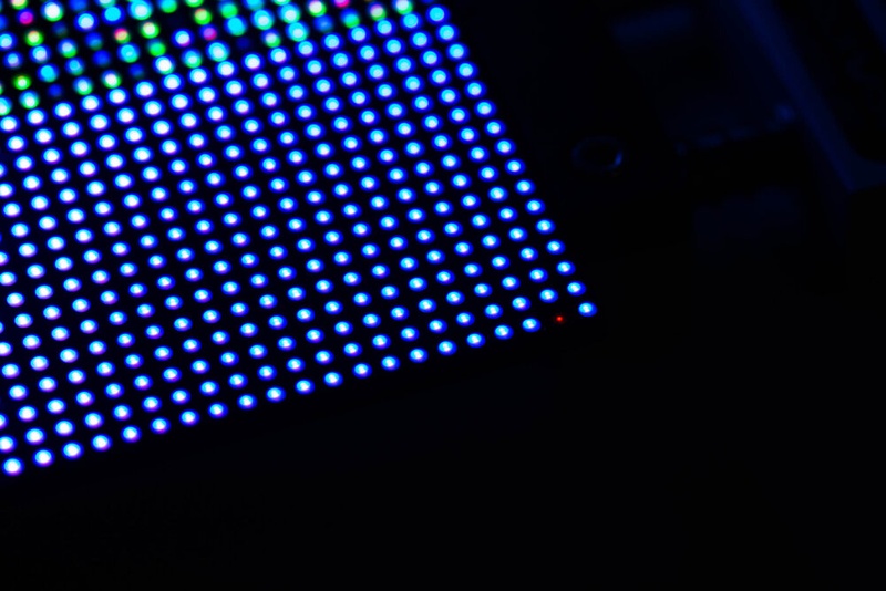
I used a stainless steel stencil and solderpaste on these boards. I didn’t want to subject the LEDs to 2 reflow cycles so I applied solderpaste and placed the controller side components first and reflowed it in my toaster oven. Then applied paste to the LED side and placed all 576 LEDs per panel. 6 in total, for 3,456 LEDs hand placed. For those interested each panel took around 2 hours to place the LEDs. I used a simple vacuum pickup tool I built for moving the LEDs from their tape into position. Having a good audio book helped here!
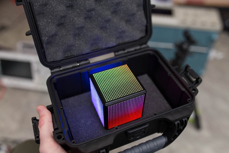
With panels designed and assembled I just need a controller and an enclosure to complete the LED Cube
Enclosure Design
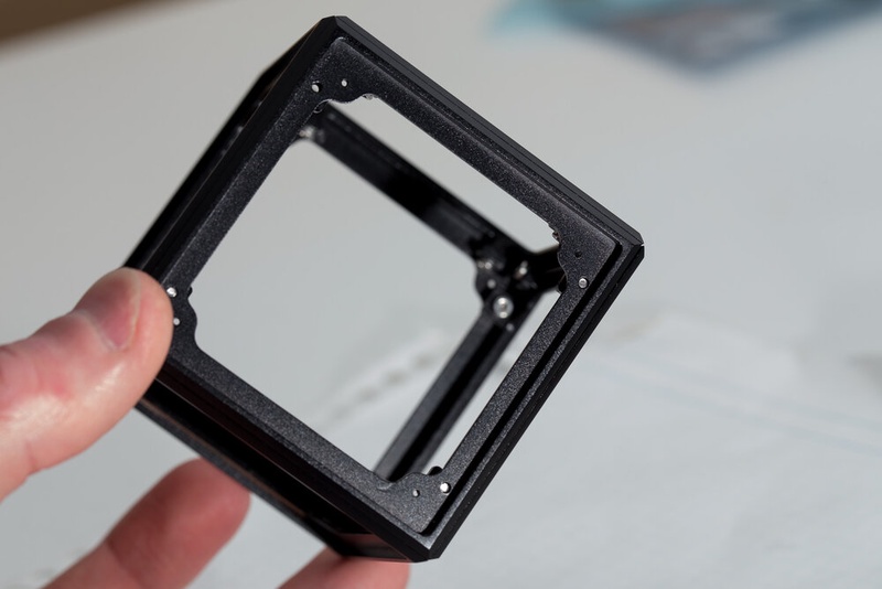
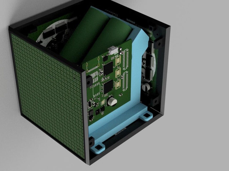
I decided I wanted to design a frame for this cube that would be made from CNC aluminium. I knew straight off the bat that my FDM printer would not be up this task, the parts will need to be very detailed and reasonably tight tolerances, and simply not suited to FDM 3d printing. After some time in Fusion 360 I had this basic design.
This design has the nice property that 6 identical pieces will fit together to create a full cube. This helps bring costs down when prototyping. With a design in hand I sent it off to the folks at NOA Labs, one of their services is prototype manufacturing. I ordered 10 pcs of the design in 6061 aluminium with black anodising. For reference including shipping this design came out to around $18 a piece. Given the complexities in shape I’m pretty happy with that cost for a fully custom prototype. About a week later I had the parts were shipped and arrived a few days after that.
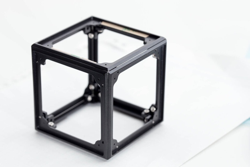
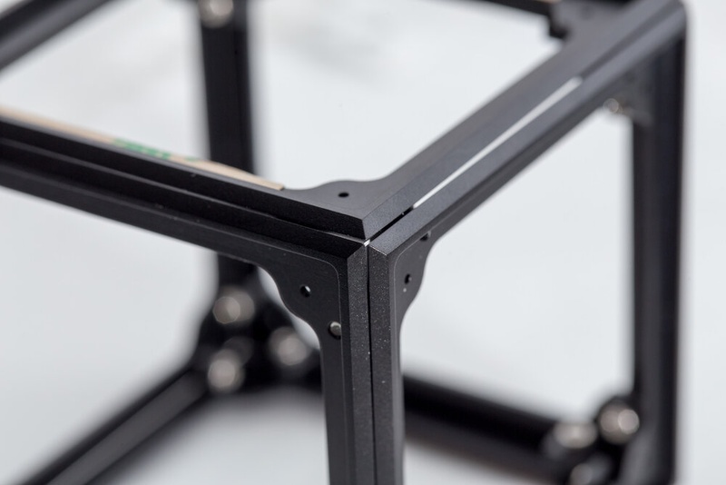
The frame was manufactured perfectly! I’m still not even sure how they managed some of the details. Some creative fixturing was probably involved. When I designed this I though the 1mm or so I had created on these bevelled edges would be tiny, but when holding it in your hands it’s quite a large edge when compared to everything else. On a second revision trying to reduce that bevel would be high on my list.
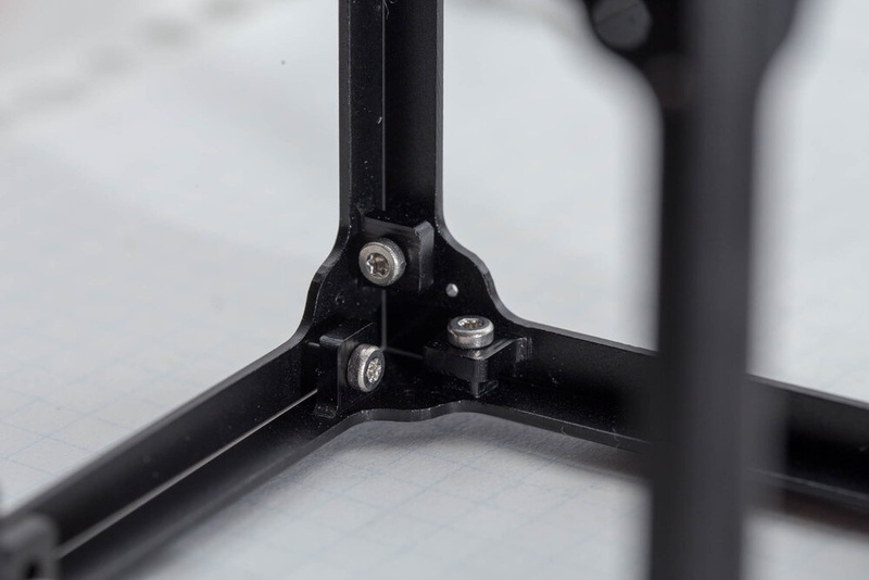
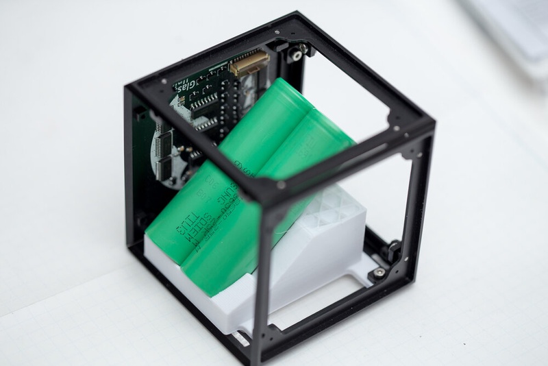
I’ve planned to modify one of the sides manually and then secure it in place using super glue and magnets, this ended up actually working surprisingly well.
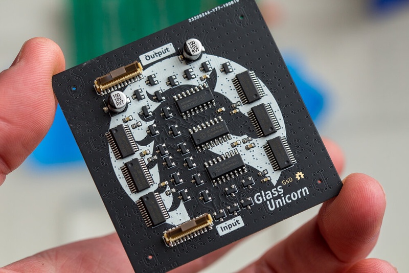
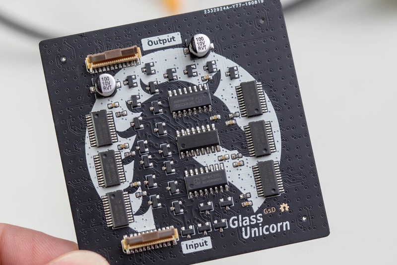
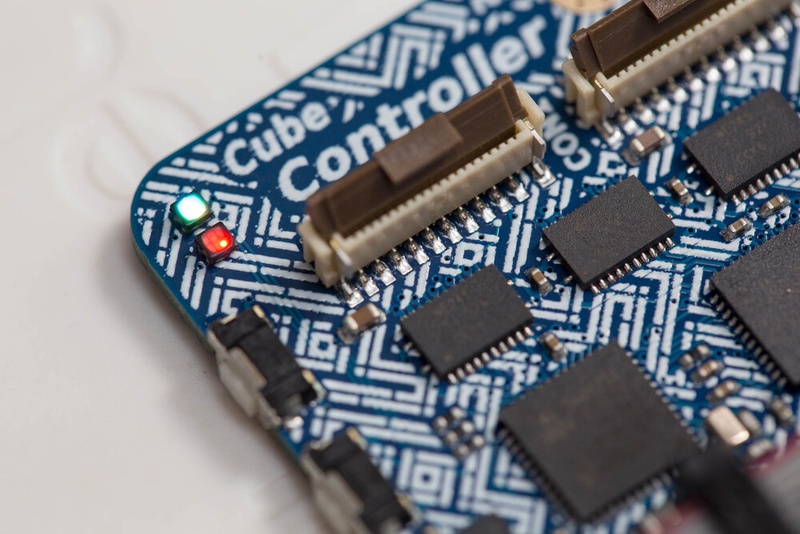
Controller
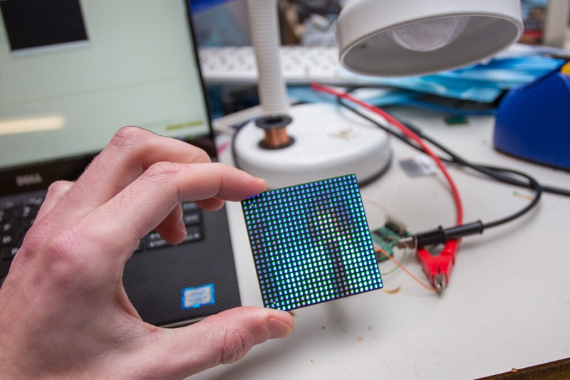
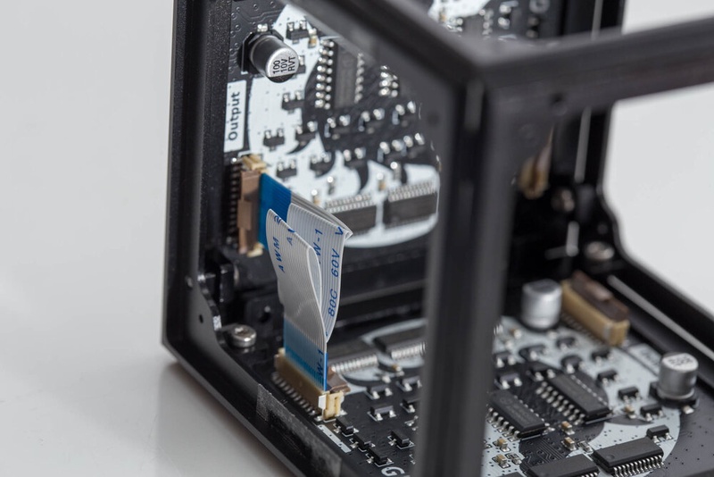
With the panels and the enclosure done, I was on the home stretch. I just needed to create a controller. The controller would sit inside and be powered from some batteries, so that the entire thing could be closed up and self powered. Up to this point I had been using the icrebreaker FPGA development board to control the panels. The gateware loaded makes use of the large SPRAM inside the ice40UP5K FPGA to create a framebuffer. This framebuffer is accessed by the internal multiplexing logic as well as a SPI listener. Perfect, I can easily replicate this circuit on a custom controller board, then add a more powerful microcontroller to calculate/generate frame data, then output this data over a SPI link to the gateware. I settled on the following architecture using a microchip SAMD51 processor. This chip can run at 120MHz and should have enough grunt to generate some pretty patterns.
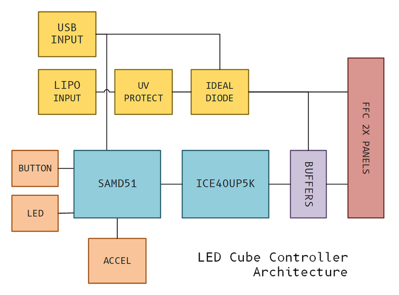
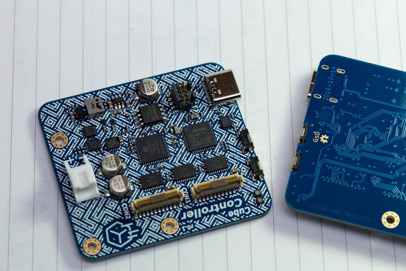
With the architecture decided I created a KiCad project, I don’t have a schematic for this because I actually used python and a library called SKiDL: https://github.com/xesscorp/skidl. It was an interesting experience and I think SKiDL and textual/generative netlists could be very useful in certain designs. For example creating the matrix of LEDs and drivers would have been a perfect use of SKiDL, maybe on my next LED design… ;)
SKiDL only replaces the schematic entry portion of a design, the routing is still handled in KiCad as usual.
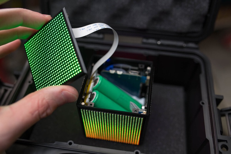
The final puzzle piece was a battery holder. I wanted to be able to take this creation to SuperCon 5 (2019), which would involve taking this through international airport security, so unprotected RC LiPo cells were out of the equation. I ended up being able to use 2x 18650 cells fitted in diagonally, this provided around 8 hours of runtime. Although my under voltage disconnect circuit was quite fiddly with its hysteresis values. So if I removed the batteries after ~5hrs it wouldn’t turn on again, even though there was plenty of power left and no chance of damaging the cells dues to over discharge.
The firmware is pretty basic, but to give myself I challenge I opted to try out embedded rust. The samd51 already has a pretty complete hal/pac crate available. So it wasn’t too difficult to get a basic firmware up and running. The tricky part was adding some basic support to the crate to support the DMA peripheral in the SAMD51 to give fast and CPU free SPI data transfers.
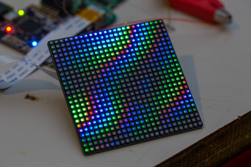
The firmware embeds the ice40 bitstream which is loaded, then a timer is started at 60Hz. Every time the timer elapses a frame is generated, I’ve been experimenting with creating patterns based on the x/y position and current time being fed through sin/cosine functions and lookup tables. DMA support was very useful in order to boost performance, it’s used by both the initial bitstream loading as well as transferring data into the framebuffer of the ice40.
Conclusion
Out of all 3,457 LEDs places, I only had 1 LED that I misplaced. After initially repairing it under hot-air it stopped working and needed to be repaired again. Every other LED worked perfectly.
Downloads/Source code
Want to build one for yourself? Grab all the sources here!
If you build one or something similar, share it with me, I’d love to see it!